

[For more diverse corporate information on the startup featured in this article, please visit the Unicorn Factory big data platform ‘Data Lab’.]
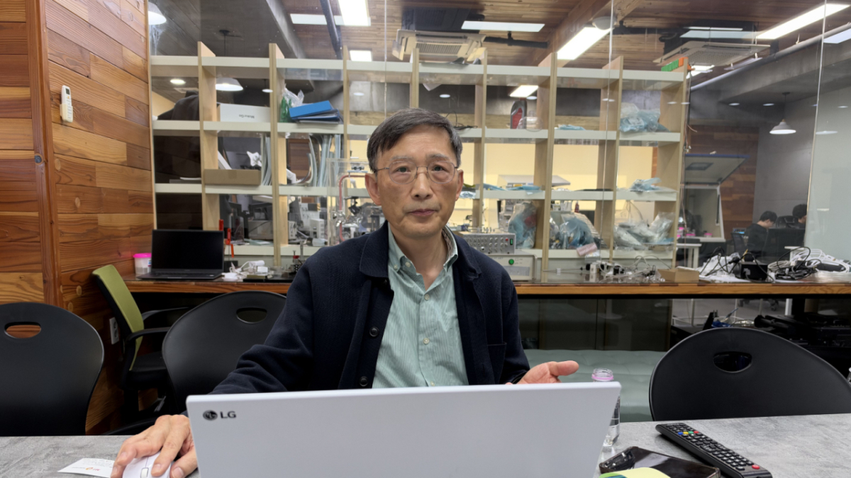
“Conventional cantilever-based atomic force microscopes are capable of 3D measurement, but they suffer from severe probe wear and slow speeds, limiting their use to research labs or sampling inspections. We will solve these problems with a quartz tuning fork (QTF)-based multi-head atomic force microscope and establish a new standard in the semiconductor metrology and inspection market.”
Je Won-ho, CEO of Multiscale Instruments (MSI) (Honorary Professor, Department of Physics and Astronomy, Seoul National University), stated this recently while explaining his company’s independently developed quartz tuning fork (QTF)-based multi-head atomic force microscope in an interview with MoneyToday’s startup media platform, ‘Unicorn Factory.’
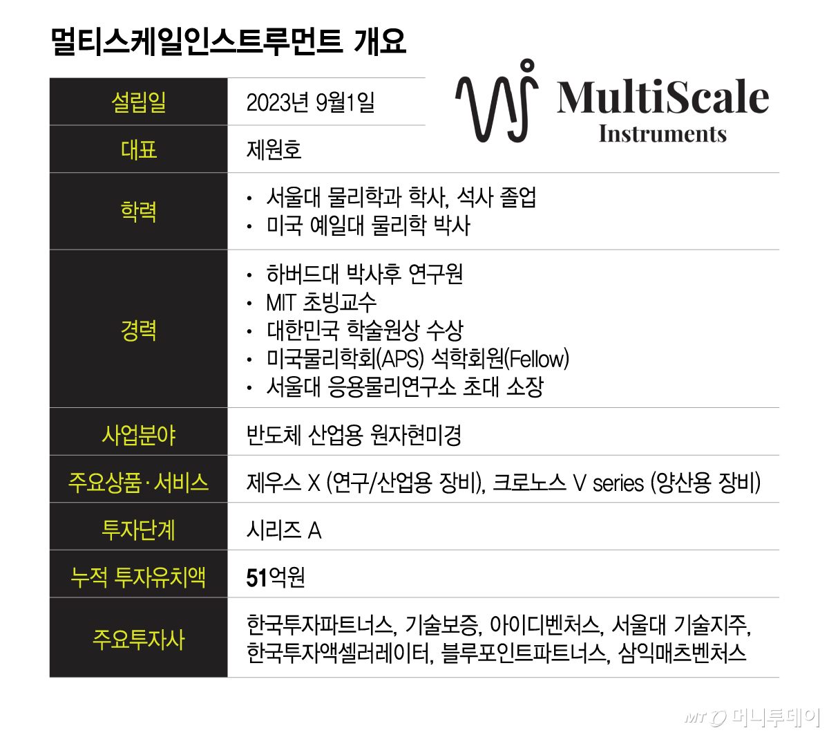
Multiscale Instruments, a second-cohort company under the ‘SNU Big Scale-up’ program of Seoul National University’s Startup Support Team, has recently secured Series A investment from Korea Investment Partners, ID Ventures, the Technology Guarantee Fund, and Seoul National University Technology Holding. The company is accelerating mass production fab validation and commercialization of its QTF-based multi-head atomic force microscope.
◇ Next-Generation Atomic Force Microscope Targeting the 3D Stacking Era in Semiconductors
As demand for rapidly processing large-scale computational data has surged due to the advancement of AI (artificial intelligence) services, the semiconductor industry is focusing on extreme miniaturization—reducing circuit widths to below 3 nanometers (nm)—and the transition to 3D (three-dimensional) packaging, such as high-bandwidth memory (HBM), which stacks chips vertically. This strategy aims to maximize power efficiency and data transmission speeds within limited areas.
The problem is that due to the nature of vertical chip stacking processes, existing inspection equipment that views surfaces from above struggles to detect vertical steps or defects. Until now, 2D scanning electron microscopes (CD-SEM) or optical inspection equipment, which fire electron beams from top to bottom to examine flat planes, have been mainstream in actual mass production lines. However, atomic force microscopes capable of 3D measurement are essential for identifying nanometer-scale vertical steps and pattern slopes.
Although cantilever-based atomic force microscopes capable of 3D measurement have been developed, they carry structural limitations for application in mass production lines. These microscopes inspect surfaces by scratching or tapping with a fine probe attached to the end of a thin plate, but the probes frequently wear out and break as they are dragged across wafers. Consequently, they have remained at the level of laboratory use or sampling inspections, failing to be applied to inline processes for real-time 100% inspection of wafers.
CEO Je pointed out that “large fabs incur monthly costs of nearly several hundred million won just for replacing cantilever probes, and their slow measurement speed makes them unsuitable for 100% inspection on mass production lines where wafers are produced in large volumes.” He added, “Due to the burden of component costs and issues with measurement reliability, global fabs have been reluctant to fully adopt atomic force microscopes until now.”
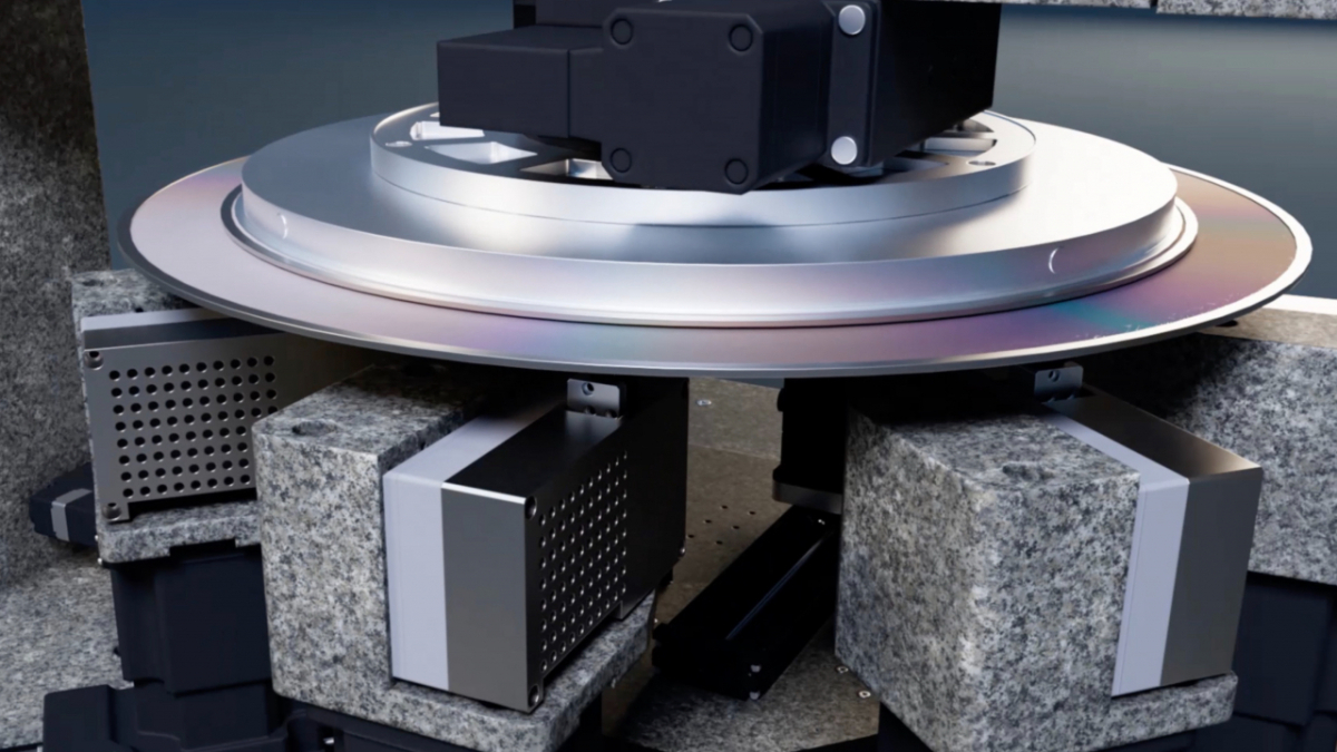
Multiscale Instruments solved these problems by utilizing the ‘hard strength’ of quartz tuning forks (QTFs), which were previously used as components in digital watches. Unlike conventional cantilever methods where probes easily bend and stick to wafers, the hard strength enables non-contact measurement without damaging the wafer. The probes can be used for over a month, and the cost is less than half that of traditional systems, reducing the financial burden.
The company has also implemented a multi-head structure that operates multiple atomic force microscopes simultaneously. It completed a prototype where eight metrology heads move independently on a 12-inch wafer and finished validation tests confirming high-resolution image measurement without heads colliding or interfering with each other’s signals. The plan is to increase the number of heads to 16, and up to 32 in the future. According to the company, even with just eight heads, it can inspect more than 120 wafers per hour, allowing for 100% inspection without slowing down mass production line speeds.
◇ Also Developing ‘Integrated Atomic Force Microscope’ That Penetrates Chamber Interiors
Multiscale Instruments is also developing an atomic force microscope that can be directly integrated into core process equipment such as semiconductor deposition, etching, and chemical mechanical polishing (CMP).
In advanced ultra-fine processes, the vacuum state breaks down the moment a wafer is removed from the chamber, delaying process time. Conversely, placing sensors inside the equipment allows for immediate detection of etch pattern slopes or surface defects without removing the wafer. CEO Je explained that for mass production lines producing 50,000 wafers per month at 3nm or below, early defect prevention can reduce annual losses ranging from 40 billion to 55 billion won, and equipment introduction costs can be recovered within six months.
CEO Je stated, “The integrated atomic force microscope, which places sensors directly inside process equipment chambers, is a unique area with no competitors in the global market.” He added, “We are currently promoting technical consultations and sample evaluations with major domestic memory manufacturers as well as global semiconductor equipment companies.”
◇ “Targeting Entry into Global Fab Mass Production Lines in 2027”
Following the start of supply for ‘Jheus X,’ a research and industrial dual-use model supporting both 8-inch and 12-inch wafers, Multiscale Instruments plans to unveil ‘Chronos V8,’ an 8-head prototype for actual mass production lines, by year-end.
The recently secured Series A investment will be focused on expanding core R&D personnel, demo rooms, and dedicated assembly facilities. The company is also fully launching its global market entry. It plans to participate in the Seoul Integrated Pavilion at ‘CES 2027,’ held in Las Vegas, USA, in January 2027, to showcase its multi-head prototype and secure global semiconductor customers.
CEO Je said, “Innovative technologies that change the world always face the prejudice of being unrealistic in their early stages.” He added, “Just as Elon Musk creates new Roadsters with SpaceX technology, it is ultimately the substance of the technology that proves the market.” He emphasized, “With our quartz tuning fork technology, we will overcome the limitations of existing atomic force microscopes and lead the next-generation AI semiconductor metrology market.”
[MoneyToday Startup Media Platform Unicorn Factory]

 in FUTURE


