

Samsung Electronics Chairman Lee Jae-yong will take the lead in commanding the groundbreaking for a semiconductor mega-project. The chairman will visit Samsung's Onyang site in Chungcheong Province alongside key executives from major affiliates to accelerate investment in an HBM (High Bandwidth Memory) packaging plant. This marks a semiconductor speed-up campaign aimed at dispelling the AI (artificial intelligence) bubble theory raised by some quarters.
According to industry sources on Thursday, Samsung Electronics is scheduled to hold a groundbreaking ceremony for an HBM advanced packaging fab at its Onyang site in Asan City, South Chungcheong Province, next week.
It is known that key executives from major affiliates will attend, including Chairman Lee, Jeon Young-hyun, head of the Device Solutions (DS) Division and Vice Chairman of Samsung Electronics, Jang Deok-hyun, president of Samsung Electro-Mechanics, Lee Cheong, president of Samsung Display, and Choi Ju-sun, president of Samsung SDI.
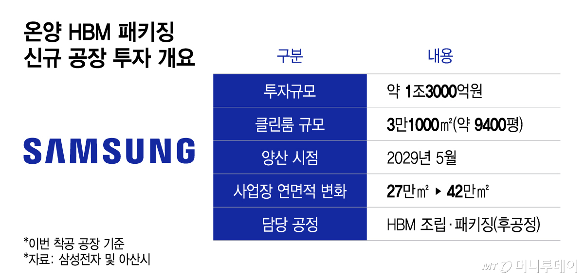
The new fab is a dedicated HBM advanced packaging facility to be newly built at the existing Onyang site. Approximately 1.3 trillion won will be invested to create a cleanroom with an area of 31,000 square meters (approximately 9,400 pyeong).
The target date for mass production is May 2029. Upon completion of the expansion, the total floor area of the Onyang site will increase from the existing 270,000 square meters to 420,000 square meters.
The Onyang site, which began as a semiconductor assembly and inspection line for Samsung Electronics in 1991, is a major back-end process hub. With this expansion, the site is expected to accelerate its transition from a back-end process hub centered on general-purpose semiconductors to a core hub for advanced HBM packaging.
Notably, this expansion is the first project to break ground nationwide among the government's "Three Major Mega-Projects for Korea's Great Leap." This signifies that the investment plan to restructure the Chungcheong region as an HBM advanced packaging hub has entered a full-fledged execution phase.
In June, at a report to the public, Lee said, "We will concentrate investments in the Chungcheong region, including Cheonan and Onyang, for HBM fabs alongside existing semiconductor back-end process fabs."
Samsung Electronics plans to invest a total of 46 trillion won in the Onyang site over the medium to long term to build five HBM fab lines.

 in INDUSTRY
