

[For more diverse corporate information on startups, please visit the Unicorn Factory big data platform 'Data Lab' .]
The performance competition in AI (artificial intelligence) semiconductors is expanding beyond chips to 'substrates.' This is because as multiple computing chips and high-bandwidth memory (HBM) are combined within a single package, the size and power consumption of semiconductor packages are increasing simultaneously.
Conventional semiconductor packages have primarily used polymer-based organic substrates. The blue or green printed circuit boards (PCBs) found inside electronic products are representative examples. However, in chips that consume significant power, such as AI semiconductors, a problem known as 'warpage,' where the substrate bends due to heat, can occur.
Furthermore, existing substrates have relatively rough surfaces, making it difficult to implement fine wiring, and signal attenuation and heat generation increase as data transmission frequencies rise. Even if the computing performance of AI semiconductors is improved, the overall system performance may degrade if the substrate that transfers data between chips cannot support it.
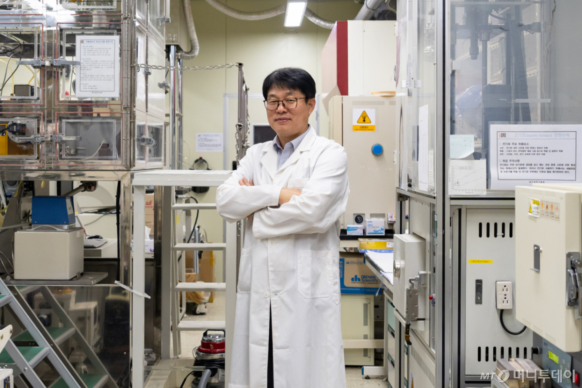
Kim Bok-hyun, Senior Researcher at the Advanced Photon Technology Research Institute, Gwangju Institute of Science and Technology (GIST), stated, "AI semiconductors consume large amounts of power, and package sizes continue to grow," adding, "Existing polymer substrates have issues with bending due to heat, leading to movements to replace them with glass substrates."
He continued, "The technology currently under development is a core material technology necessary for replacing the organic material substrates of existing semiconductors with special glass substrates," noting, "It can be viewed as a next-generation substrate aimed at enhancing the performance and power efficiency of AI semiconductors."
'Low-Dielectric Glass' Different from Window Glass… Reduces Signal Attenuation and Heat Generation
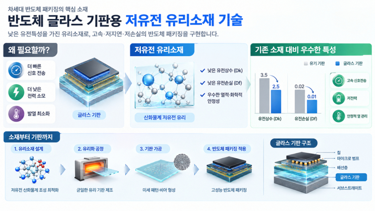
Glass substrates for semiconductors differ from ordinary glass used in windows or displays. They are special glass with reduced dielectric constant and dielectric loss, enabling high-frequency electrical signals to be transmitted quickly and without loss.
The dielectric constant (Dk) indicates the degree to which a material polarizes in response to an electric field. A high dielectric constant can affect signal transmission speed and delay. Dielectric loss (Df) refers to the extent to which the energy of electrical signals is dissipated as heat within the material.
If these two values are high, high-speed data signals traveling along copper wiring on the substrate may weaken, potentially increasing noise and heat generation. In particular, as the frequency used for data transmission rises above 10 to 20 gigahertz (GHz), the dielectric properties of glass materials become increasingly important.
Researcher Kim explained, "Copper wiring is formed on semiconductor substrates, and high-speed data signals pass over it," adding, "If the dielectric constant or dielectric loss of the substrate material is high, signals attenuate, causing noise and heat generation."
He further stated, "Glass substrates for semiconductors are not simply transparent and hard glass," noting, "They are special glass that must possess low-dielectric properties, thermal expansion characteristics, mechanical strength, and processability simultaneously."
Researcher Kim's team improved dielectric properties and thermal stability by adjusting the composition of aluminoborosilicate glass. Aluminoborosilicate glass is a type of glass with silicon dioxide, boron oxide, and aluminum oxide as its basic components.
Connecting with Light Instead of Copper Wiring… Expansion to Optical Interconnects
The glass developed by the research team focused on reducing losses and heat generation that occur when high-speed data signals pass through the substrate. Unlike methods that repurpose existing display glass for semiconductor substrates, its feature is that the composition and internal structure of the glass were designed from the outset to suit high-performance semiconductor packaging.
It was not just electrical performance that was improved. The material was engineered to expand and contract at a level similar to silicon chips even when temperatures change, reducing the possibility of substrate bending or cracks forming in joints. Thermal stability was also enhanced to withstand the high temperatures and micro-processing involved in semiconductor manufacturing processes.
Researcher Kim stated, "Semiconductor substrates must possess signal transmission performance, thermal expansion characteristics, strength, and processability," adding, "The team differentiated itself by securing multiple physical properties in a balanced manner so that they could be applied to actual semiconductor processes, rather than maximizing just one performance metric."
He continued, "A low dielectric constant alone does not make a good semiconductor substrate material," noting, "It must match the thermal expansion characteristics of silicon, remain undeformed during high-temperature processes, and withstand processes that involve drilling holes in the substrate and forming wiring."
Another advantage of glass substrates is that channels for light to pass through can be created internally. The research team plans to expand this technology into 'optical interconnects.' In the case of existing copper wiring connecting chips, power consumption and signal loss increase as data throughput and transmission distance grow.
Optical interconnect is a technology that converts part of electrical signals into optical signals for transmission. By forming an Optical Waveguide with a different refractive index inside the glass, light can travel along a predetermined path. It is akin to creating a 'highway for light' within the glass instead of copper wiring.
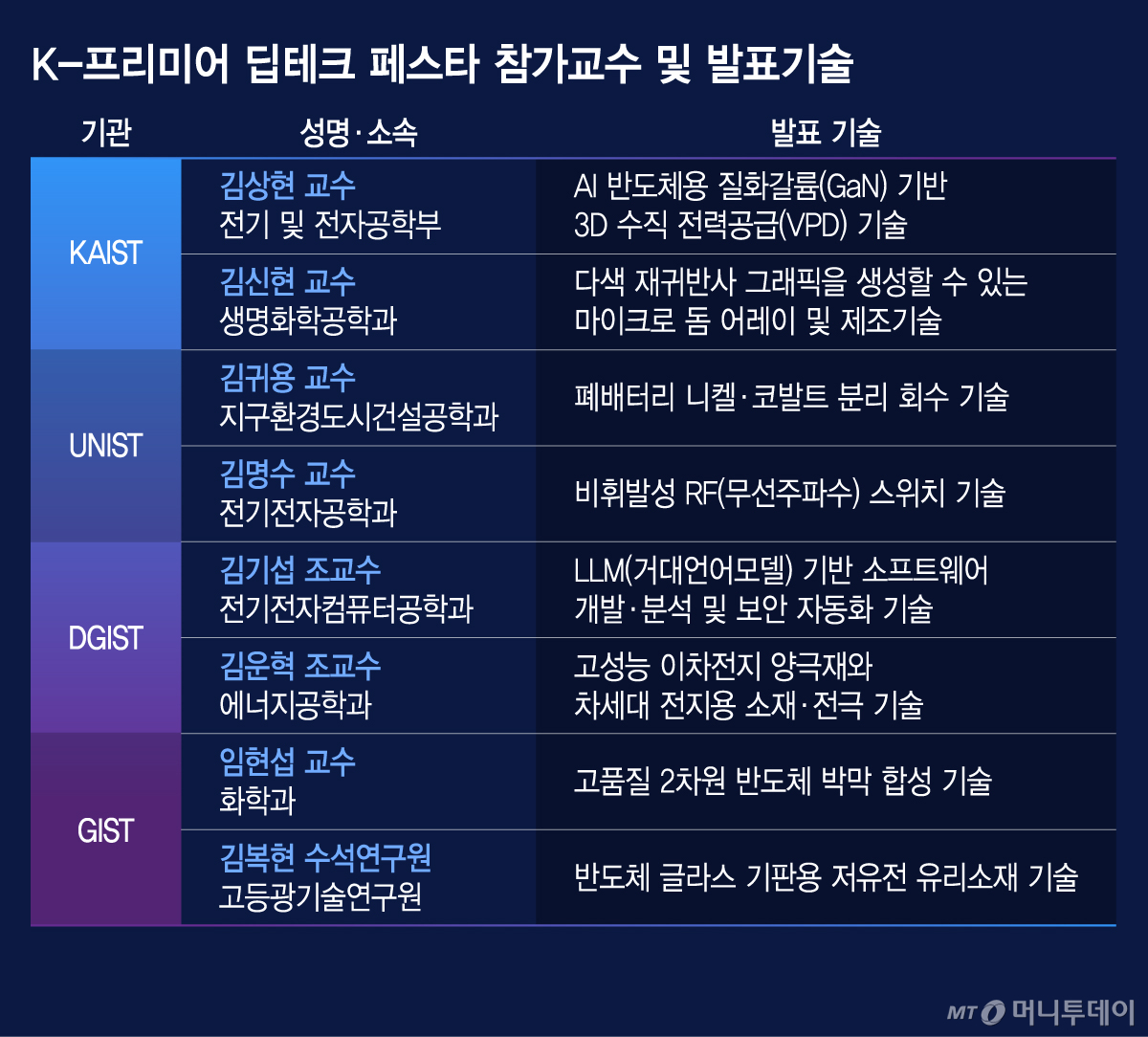
Researcher Kim will introduce related technologies at the '2026 K-Premier Deep Tech Festa' (Registration: https://vvd.bz/buvX ), to be held on the 29th in Hall B Plus Stage of COEX in Samsung-dong, Seoul.
He stated, "I would like to collaborate with semiconductor package companies such as Samsung Electro-Mechanics that require optical interconnect technology, and optical transceiver companies such as OUI Solutions," adding, "The key to commercialization is understanding the structures and detailed specifications desired by end-demand companies and jointly optimizing material and optical waveguide technologies."
<Registration for 'K-Premier Deep Tech Festa (Technology Transfer and Commercialization)' >
- Date: October 29, 2026 (Thu), 1:00 PM
- Location: Hall B PLUS STAGE, COEX, Samsung-dong, Seoul
- Target Participants: Companies considering technology transfer, joint research, or new business ventures; family companies of government-funded research institutes; investment firms
- Participation Fee: Free (Advance registration required)
- Hosts: Ministry of Science and ICT, KAIST, GIST, DGIST, UNIST, MoneyToday Unicorn Factory
- Sponsors: Korea Institute of Science and Technology Information (KISTI), Commercialization Promotion Agency for R&D Outcomes (COMPA)
- Application: https://vvd.bz/buvX
[MoneyToday startup media platform 'Unicorn Factory' ]

 in FUTURE


