

[For more diverse corporate information on startups, visit the Unicorn Factory Big Data Platform 'Data Lab'.]
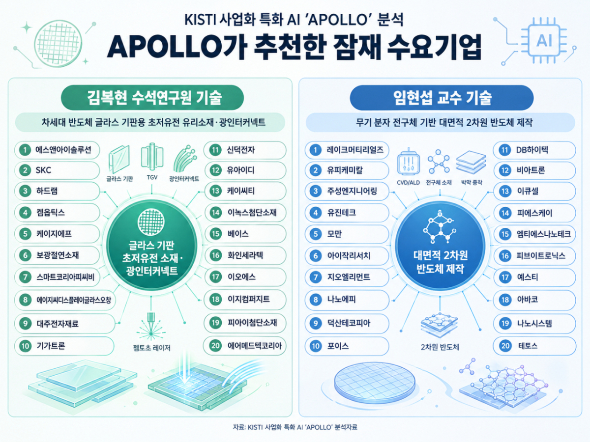
The ultra-low dielectric glass material for next-generation semiconductors and the large-area two-dimensional (2D) semiconductor synthesis technology developed by the Gwangju Institute of Science and Technology (GIST) have been recognized for their commercialization potential in the AI (artificial intelligence) and high-performance computing (HPC) semiconductor markets.
The Technology Commercialization Research Center at the Korea Institute of Science and Technology Information (KISTI) analyzed the research outcomes of Senior Researcher Kim Bok-hyun at GIST's Advanced Light Technology Institute and Professor Im Hyun-seop in GIST's Department of Chemistry using its self-developed commercialization-specialized AI, "Apollo," and derived these results.
The two researchers are scheduled to introduce the technologies directly at the "2026 K-Premier Deep Tech Festa" (Registration: https://vvd.bz/buvX), which will be held on the 29th in Hall B of COEX in Seoul Samsung-dong. Following their presentations, they will conduct individual consultations with companies interested in proof of concept (PoC), technology transfer, or commercialization.
Apollo is a commercialization-specialized AI that analyzes over 370 million data points from national R&D (research and development) and patents to identify companies highly likely to require specific research outcomes. When researchers input project details, patents, or technical materials, the system analyzes characteristics and application markets, presenting potential demand-side companies along with the rationale for recommendations.
In this analysis, Apollo was first used to screen domestic potential demand-side companies. For overseas firms, KISTI utilized its global company exploration model under development to compare patent and technology development trends between leading and follower companies, predicting the technological fields in which follower companies are highly likely to enter in the future.
"Ultra-Low Dielectric Glass Substrate" Reduces Heat and Signal Loss in AI Semiconductors
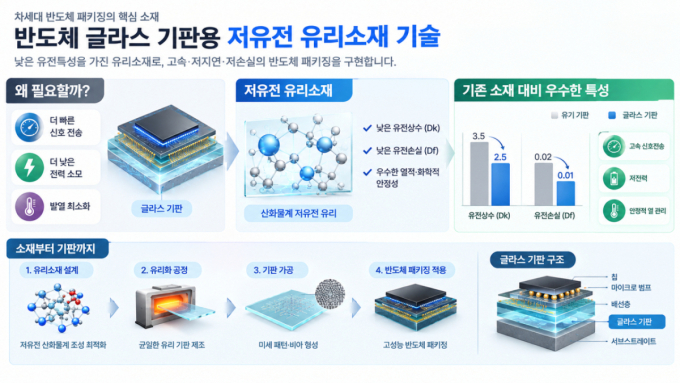
The technology developed by Senior Researcher Kim Bok-hyun is an ultra-low dielectric glass material that reduces signal loss and heat generation in glass substrates for AI semiconductors.
AI semiconductors combine multiple computing chips and high-bandwidth memory (HBM) within a single package, causing both the size of the package and power consumption to increase. Existing polymer-based organic substrates can suffer from "warping" caused by heat, and their relatively rough surfaces make it difficult to implement fine wiring.
As data transmission frequencies increase, signal attenuation and heat generation also rise. Researcher Kim's team developed a glass material capable of reducing signal loss in high-frequency environments of 30 gigahertz (GHz) or higher by adjusting the composition of aluminoborosilicate glass.
Apollo identified the semiconductor packaging substrate market as the domestic target market for this technology. It recommended companies in the fields of through-glass via (TGV), precision laser processing, optical waveguides, low-dielectric glass fiber, and printed circuit boards (PCB) as domestic firms with high potential for utilization.
A prominent candidate is "S&I Solution." This company holds technologies related to glass interposers embedded with RF communication chips and TGVs, and was evaluated as a demand-side company capable of directly verifying ultra-low dielectric glass and optical interconnect technologies.
Additionally, AI-based inspection equipment company "Hardram," "Kem Optics" equipped with optical waveguide and optical transceiver technologies, along with △CGF, △Bogwang Insulating Materials, △Smart Korea PCB, △SKC, △Daeju Electronic Materials, △Gigatron, △Sindeuk Electronics, △UID, △KCT, and △Inots Advanced Materials were recommended as potential demand-side and collaboration partners.
Apollo classified the U.S.-based Corning and Japan's Hoya as global leading companies in related technologies. It selected the U.S.-based "Absolics" and China's "Hebei Guangxing Semiconductor" as technology follower companies and potential collaboration candidates.
Large-Area 2D Semiconductors Overcoming Silicon Limitations
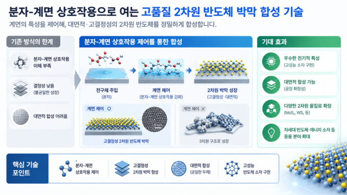
The Lim Hyeon-seop (Prof.) research team developed a technology to uniformly synthesize atomically thin 2D semiconductor thin films on large-area substrates using inorganic molecular precursors.
As semiconductor processes shrink to below the 2nd-nanometer (nm) level, limitations are emerging in precisely controlling current with existing silicon channels. This is because as channels become thinner at the atomic scale, leakage current and heat generation increase, potentially degrading device performance.
Professor Im's technology enables the precise synthesis of large-area, high-crystallinity 2D semiconductors by controlling the characteristics of semiconductor interfaces (fine boundary regions). Its feature lies in enhancing process reproducibility by understanding the interaction between precursors and substrates at the molecular level, going beyond simply repeating various conditions to find optimal values.
Apollo analyzed that this technology can produce large-area 2D semiconductor thin films with excellent crystallinity in a shorter time than existing processes, making it applicable to next-generation thin-film transistors and monolithic 3D semiconductor manufacturing.
Potential demand-side companies recommended include precursor material firms, CVD (chemical vapor deposition) and ALD (atomic layer deposition) equipment manufacturers, and device/process demonstration companies. Specifically, these include △Lake Materials, △UP Chemical, △Jusung Engineering, △Eugene Tech, △Moman, △Geo Element, △Force, △DB Hitek, and △PSK.
Additionally, △Isaac Research, △Nano Epi, △Deoksan Tecpia, △Viatron, △EQ Cell, △MTS Nano Tech, △Pbitronics, △YST, △Avaco, △Nano System, and △TeToss were presented as potential demand-side and collaboration partners.
Apollo mentioned Japan's Kokusai Electric, Ulvac, and Tokyo Electron; the U.S.'s Lam Research, Veeco Instruments, and Entegris; Germany's Aixtron; and the Netherlands' ASM International as global leading companies in thin-film deposition and precursor fields.
<Registration for 'K-Premier Deep Tech Festa (Technology Transfer & Commercialization)'>
- Date: October 29, 2026 (Thu), 1:00 PM
- Location: COEX Hall B PLUS STAGE, Seoul Samsung-dong
- Participants: Companies considering technology transfer, joint research, or new business ventures; family companies of government-funded research institutes; investment firms
- Fee: Free (Advance registration required)
- Hosts: Ministry of Science and ICT, KAIST, GIST, DGIST, UNIST, MoneyToday Unicorn Factory
- Sponsors: Korea Institute of Science and Technology Information (KISTI), Korea Commercialization Agency for Science and Technology (COMPA)
- Application: https://vvd.bz/buvX
[MoneyToday Startup Media Platform 'Unicorn Factory']

 in FUTURE


