

Curing AI Semiconductor Power Waste… This Technology Boosts Transmission Efficiency from '50% to 95%'
Professor Kim Sang-hyun, Department of Electrical Engineering, KAIST (Korea Advanced Institute of Science and Technology)
Development of gallium nitride-based technology to reduce energy waste in AI chips
"Accelerating commercialization through technology transfer… also considering direct startup"
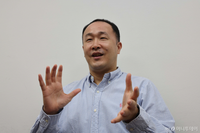
"The competition in AI semiconductors is often thought to hinge on 'who can calculate faster,' but the real decisive battleground is how efficiently electricity is supplied to the chip."
These are the words of Professor Kim Sang-hyun of the Department of Electrical Engineering at KAIST (Korea Advanced Institute of Science and Technology). The power consumed by AI semiconductors is growing steadily. In an era where a single chip uses 1-kilowatt-class power, a significant amount of energy is lost even in the process of delivering electricity to the chip. Professor Kim explained that 30% to 40% of total power can be lost during the transmission process, and if chip power consumption continues to rise, losses could reach half.
While attention has focused on increasing the calculation speed of semiconductors, energy waste generated in the process of delivering electricity has received relatively little attention. Professor Kim found solutions in semiconductor structures and gallium nitride (GaN) materials that he has been researching for some time.
To reduce power loss, the method of sending electricity must change first. Even when sending the same amount of power, lower voltage requires more current to flow, generating heat in wires and components, which wastes energy. This is also why power plants send electricity at high voltage and step down the voltage near consumption sites.
AI servers are no different. Electricity entering a server goes through multiple stages to be converted into a low voltage of around 1 volt that the chip can use. The problem is that devices for lowering voltage have traditionally been placed horizontally next to the chip, at a distance. The longer the distance from where the voltage is lowered to the chip, the greater the inevitable loss.
Professor Kim's team solved this problem by placing the voltage-lowering device vertically directly beneath the chip. Simply put, electricity is sent to under the chip at high voltage, and then the voltage is lowered there for immediate supply. The principle minimizes energy loss by shortening the distance electricity travels in a low-voltage state.
The material playing a key role in this process is 'gallium nitride' (GaN). Lowering voltage requires switches that rapidly turn electricity on and off, where higher resistance causes electricity to convert into heat, resulting in energy loss. Professor Kim explained that gallium nitride offers advantages in reducing power loss by lowering resistance compared to conventional silicon.
Professor Kim's team announced that applying this technology can boost the efficiency of delivering power to the chip from the existing 50% range to 85-95%. Professor Kim said, "The more power a single chip consumes, the more power can be saved."
The research achievements of Professor Kim's team have been accepted multiple times at IEDM and VLSI Symposiums, major international academic conferences in the semiconductor device field. This signifies that the originality and technical potential of the research have been recognized by the international academic community.
Professor Kim stated, "Until 1 or 2 years ago, there were hardly any places conducting similar research, but recently related research is rapidly increasing in China, which has strong gallium nitride technology capabilities," adding, "Among companies, Intel, which has developed CPUs (Central Processing Units) for servers for a long time, is moving the most actively."
The biggest challenge to be solved for commercialization is mass production. Currently, semiconductor chips responsible for computation and devices that regulate voltage must be manufactured using different processes and then combined. This is because the chip must be produced with existing silicon processes, while the voltage regulation device must be produced with gallium nitride processes. It also requires further optimization of how to connect the two components and where to place the components necessary for stable power supply.
In particular, a stumbling block is that foundries (semiconductor contract manufacturing companies) do not yet sufficiently support the processes required for this technology. Professor Kim said, "The short-term goal is to first prove performance in university laboratories to guide foundries toward developing related processes," adding, "We also plan to conduct follow-up research to verify actual effects across the entire circuit and system."
Commercialization will initially be pursued through technology transfer. This judgment stems from the belief that if companies interested in the technology take over the research results and continue development, commercialization speed can be increased. If technology transfer alone cannot ensure the level of completeness desired by companies, faculty-led startups are also being considered. Professor Kim said, "Companies want sufficiently verified technology, but if there is a large gap between the technology secured in the laboratory and the level desired by companies, starting a business directly to further develop the technology is also an option."
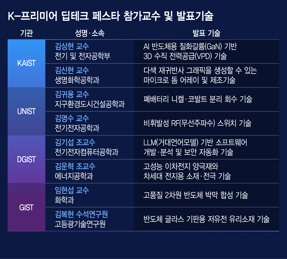
Professor Kim plans to introduce this technology at the '2026 K-Premier Deep Tech Festa' to be held on the 29th at Hall B of COEX in Samsung-dong, Seoul. He said, "I want to meet chip manufacturers and packaging companies as cooperative partners." This is because placing the voltage regulation device directly beneath the chip requires supporting packaging technology that combines the two components into one.
New Technology Producing Color Without Dyes… Aiming Beyond Anti-Counterfeiting to the Art Market
Professor Kim Shin-hyun, Department of Biological and Chemical Engineering, KAIST (Korea Advanced Institute of Science and Technology)
Gaining attention for developing structural color technology free from environmental and fading concerns
"Diverse applications from anti-counterfeiting to art materials"
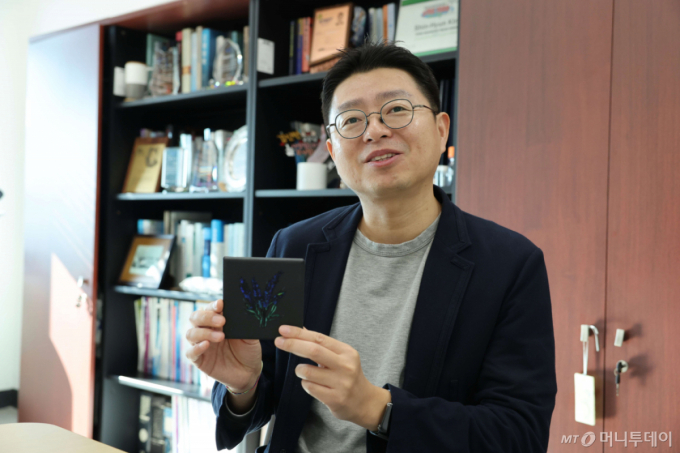
Pictures printed on paper and paint on building exteriors fade over time. This is because chemical pigments that produce color undergo changes in molecular structure when exposed to ultraviolet rays for long periods.
Professor Kim Shin-hyun of the Department of Biological and Chemical Engineering at KAIST (Korea Advanced Institute of Science and Technology) solved this problem with 'structure' rather than pigment. Simply put, he etches hemispherical microstructures at a scale one-tenth the thickness of a hair into transparent materials that have no color themselves to produce color. Professor Kim said, "As long as the structure is maintained, the color lasts permanently, eliminating concerns about fading," adding, "It also reduces environmental issues and human toxicity associated with the pigment synthesis process, making it significant from a sustainability perspective."
Structural color refers to colors that appear when regular structures inside a substance interfere with light, such as on the wings of morpho butterflies or in opals. Even with the same material, changing only the structure can produce various colors.
Professor Kim has focused exclusively on structural color research for over 20 years since his student days. Existing technology that arranges particles of 100 nanometers (nm) in three dimensions was developed together with the Korea Minting and Security Printing Corporation and has already been applied to products such as Gangwonland casino chips. However, the process is delicate, and while creating a single color pattern is easy, it is difficult to create intricate graphics with mixed colors.
The new technology changed the way color is created from the start. Professor Kim said, "Unlike existing methods that mimic nature, we used principles not found in the natural world." This technology utilizes an inverted form of small hemispheres with a diameter of around 10 micrometers (µm). When light enters the side of the hemisphere, it reflects along the round surface and returns. At this time, light traveling different paths meets and interferes, producing a specific color. There is no need to use separate pigments or materials to change the color. Changing only the size of the hemisphere can create different colors. Mixing and arranging hemispheres of different sizes allows for much more diverse colors, similar to mixing paints.
The production utilizes processes used in semiconductor manufacturing. First, micro-pillars are made using a polymer that reacts to ultraviolet light, then heat is applied. As the polymer melts down, the surface becomes round, forming a hemispherical shape. The advantage is that the size and position of the hemispheres can be designed in advance, allowing desired colors to be realized at desired locations with a single process.
The research team used this technology to reproduce the Joseon Dynasty's 'Ilwolobongdo' (Sun, Moon, and Five Peaks) on a nail-sized scale. The resolution is comparable to the latest LED displays, and it can also be projected onto large screens. It also possesses 'Janus' characteristics where color is visible from one direction only, while appearing transparent from the opposite side. Professor Kim explained, "The biggest feature is that high-resolution color graphics, which were difficult with existing technology, can be created using structural color alone." This research, in which Researcher Son Chae-rim participated as the first author, was published in the international academic journal 'Advanced Materials' last February.
Professor Kim stated that structural color should find its own unique market rather than directly replacing chemical pigments. This is because the color principle differs, resulting in a different feel to the colors. While stating that it was not developed for specific uses, he cited several applications. For example, since the color changes depending on the viewing angle and microscopic text invisible to the naked eye can be engraved, it can be used as an anti-counterfeiting material for authenticity verification. Leveraging its characteristic of precisely controlling light paths, it can also be applied to optical devices or sensors.
Professor Kim said, "It is not a scientific expression, but when you actually see it, it is truly beautiful," adding, "It suits premium packaging requiring a luxurious feel, interior items, goods, and vehicle interior materials."
The technology transfer field Professor Kim personally looks forward to most is the art industry. This involves creating nail-sized works using structural color instead of paint, and then viewing them by magnifying with a microscope or projecting them onto walls for exhibition. Professor Kim said, "It can become a new form of art genre that did not exist before," adding, "We are also considering ways to collaborate with artists in the future." Since each work requires different micro-structure design, it is expected to have value as limited-edition art works differentiated from mass-produced products.
The remaining challenges are finding commercialization partners and building a Yangsan system. Unlike artworks, mass production is key for packaging and security materials. Professor Kim revealed, "It is difficult for the university alone, and it is important to find companies truly interested in the technology and move forward together." Fortunately, he explained that the process is similar to micro-lens arrays, which are already mass-produced as display films, so the Yangsan threshold is relatively low. This is a technology worth watching for security printing, display, cosmetics, luxury packaging companies, entertainment companies making photocard goods, and smart car companies. Professor Kim plans to introduce this technology directly at the 'K-Premier Deep Tech Festa' to be held on the 29th at the Plus Stage in Hall B of COEX in Seoul.
<Application for 'K-Premier Deep Tech Festa (Technology Transfer and Commercialization)'>
- Date: October 29, 2026 (Thu) 1:00 PM
- Location: Hall B PLUS STAGE, COEX, Samsung-dong, Seoul
- Participants: Companies considering technology transfer, joint research, and new businesses, government-funded research institute family companies, investment firms
- Participation Fee: Free (Pre-registration required)
- Hosts: Ministry of Science and ICT, KAIST, GIST, DGIST, UNIST, MoneyToday Unicorn Factory
- Sponsors: Korea Institute of Science and Technology Information (KISTI), Commercialization Promotion Agency for Small and Medium Technology (COMPA)
- Application: https://vvd.bz/buvX
[MoneyToday Startup Media Platform Unicorn Factory]

 in FUTURE


