

The "electricity-eating horse" of AI semiconductors: Taming heat and losses... What is this "special glass substrate"?
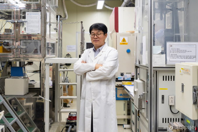
Kim Bok-hyun, Senior Researcher at the Advanced Photon Technology Research Institute, Gwangju Institute of Science and Technology (GIST)
Development of 'Low-Dielectric Glass Material Technology for Semiconductor Glass Substrates'
Replacing copper wiring with light: Expansion via optical interconnects
The performance competition in AI (artificial intelligence) semiconductors is expanding beyond chips to substrates. This is because as multiple computing chips and high-bandwidth memory (HBM) are integrated into a single package, the size and power consumption of semiconductor packages are increasing simultaneously.
Existing semiconductor packages have primarily used polymer-based organic substrates. The blue or green printed circuit boards (PCBs) visible inside electronic devices are a representative example. However, in chips that consume large amounts of power, such as AI semiconductors, the "warpage" problem can occur, in which heat causes the substrate to bend.
In addition, existing substrates have relatively rough surfaces, making it difficult to implement fine wiring, and as data transmission frequencies increase, signal attenuation and heat generation become more pronounced. Even if the computational performance of AI semiconductors is improved, if the substrate that transfers data between chips cannot support this, the overall system performance may decline.
Kim Bok-hyun, a senior researcher at the Gwangju Institute of Science and Technology (GIST) Advanced Photonics Research Institute, stated, "AI semiconductors consume significant power and their package sizes continue to grow." He added, "Existing polymer substrates have issues with warping due to heat, leading to movements to replace them with glass substrates."
He added, "The technology currently under development is a core material technology required to replace the organic substrate of existing semiconductors with a special glass substrate. It can be viewed as a next-generation substrate aimed at enhancing the performance and improving the power efficiency of AI semiconductors."
Glass substrates for semiconductors are different from ordinary glass used in windows or displays. They are a special type of glass with reduced dielectric constant and dielectric loss, enabling high-frequency electrical signals to be transmitted quickly and without loss.
The dielectric constant (Dk) indicates the degree to which a material becomes polarized in response to an electric field. A high dielectric constant can affect signal transmission speed and delay. The dielectric loss factor (Df) measures the extent to which the energy of an electrical signal is dissipated as heat within the material.
When these two values are high, high-speed data signals traveling along the copper wiring on the substrate can weaken, and noise and heat generation may increase. In particular, as the frequency used for data transmission rises to 10–20 gigahertz (GHz) or higher, the dielectric properties of glass materials become increasingly important.
Researcher Kim Bok-hyun explained, "Copper wiring is formed on top of semiconductor substrates, and high-speed data signals travel over it. If the dielectric constant or dielectric loss of the substrate material is high, signal attenuation occurs, leading to noise and heat generation."
He added, "Glass substrates for semiconductors are not simply transparent and hard glass. They are a special type of glass that must simultaneously possess low dielectric properties, thermal expansion characteristics, mechanical strength, and processability."
Researcher Kim's team improved the dielectric properties and thermal stability of aluminoborosilicate glass by adjusting its composition. Aluminoborosilicate glass is a type of glass whose basic components include silicon dioxide, boron oxide, and aluminum oxide.
The research team developed the glass with a focus on reducing signal loss and heat generation that occur when high-speed data signals pass through a substrate. Unlike approaches that repurpose existing display glass for use as semiconductor substrates, the key feature of this development is that the glass composition and internal structure were designed from the outset specifically for high-performance semiconductor packaging.
It is not merely an improvement in electrical performance. The material has been engineered to expand and contract at a level comparable to that of silicon chips even as temperature changes, thereby reducing the likelihood of substrate warping or cracks forming at junctions. Thermal stability has also been enhanced so that it can withstand the high temperatures and microfabrication processes involved in semiconductor manufacturing.
Researcher Kim stated, "Semiconductor substrates must possess signal transmission performance, thermal expansion characteristics, strength, and processability all at once," adding, "The research team differentiated its work by securing a balanced set of physical properties suitable for application in actual semiconductor manufacturing processes, rather than maximizing any single performance metric."
He added, "A low dielectric constant alone does not make a material suitable as a semiconductor substrate. It must match silicon in terms of thermal expansion characteristics, remain undistorted during high-temperature processes, and withstand the processes of drilling holes in the substrate and forming wiring."
Another advantage of glass substrates is that they can create pathways for light to travel through internally. The research team plans to expand this technology into "optical interconnects." In the case of existing copper wiring connecting chips, power consumption and signal loss increase as data throughput and transmission distance grow.
Optical interconnect is a technology that converts part of an electrical signal into an optical signal for transmission. By forming optical waveguides with different refractive indices inside glass, light can travel along a predetermined path. This effectively creates a "highway for light" within the glass, replacing copper wiring.
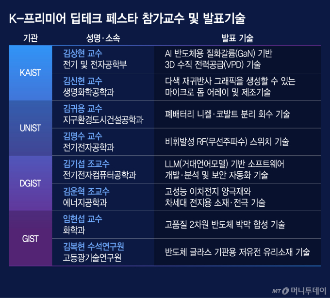
Researcher Kim will introduce the related technology at the "2026 K-Premier Deep Tech Festa," which will be held on the 29th at the Plus Stage in Hall B of COEX in Seoul Samsung-dong (Registration: https://vvd.bz/buvX).
He stated, "I would like to collaborate with semiconductor packaging companies such as Samsung Electro-Mechanics that require optical interconnect technology, and optical transceiver companies such as OUI Solutions." He added, "The key to commercialization lies in understanding the structures and detailed specifications desired by end users, and jointly optimizing the materials and optical waveguide technology accordingly."
“It’s Time to Change the Materials for Semiconductors, Too”... “2D Materials” That Will Overcome the Limits of Silicon
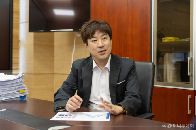
Im Hyun-seop, Professor in the Department of Chemistry at Gwangju Institute of Science and Technology (GIST)
Development of 'High-Quality Two-Dimensional Semiconductor Thin Film Synthesis Technology'
Large-area production possible... Green light for next-generation semiconductors
The semiconductor industry has improved performance by making transistors (semiconductor devices that function as electrical switches and voltage amplifiers) smaller. This approach involves integrating more transistors onto a single chip to increase computing speed while reducing power consumption.
However, as semiconductor processes shrink to below the 2nd-nanometer (nm) level, the focus has shifted from "how small can it be made" to "what materials should be used."
This is because as the "channel," which serves as the pathway for current flow inside a transistor, becomes thinner at the atomic level, it becomes difficult to precisely control the current using conventional silicon materials. This can also lead to issues such as increased leakage current and heat generation, as well as degraded device performance.
Im Hyun-seop, a professor in the Department of Chemistry at GIST (Gwangju Institute of Science and Technology), stated, "As semiconductor processes continue to shrink, we are reaching physical limits in improving performance using silicon." He added, "Ultimately, the material used for the channel must be replaced with a better one."
Two-dimensional (2D) semiconductors, which are only a few atomic layers thick, are cited as candidates to replace or complement silicon. A representative material is molybdenum disulfide (MoS₂). MoS₂ has a sandwich structure in which molybdenum atoms are situated between sulfur atoms. It possesses a band gap—the energy interval that allows current to be switched on and off—despite having a thickness of less than 1 nanometer.
Graphene is also a representative two-dimensional material, but its near-zero band gap limits its use as a channel for digital semiconductors. In contrast, transition metal dichalcogenides (TMDs) such as molybdenum disulfide (MoS₂), tungsten disulfide (WS₂), and tungsten diselenide (WSe₂) retain their semiconducting properties even at the atomic layer thickness.
The explanation is that the thinness of the material makes it advantageous for the gate to control the current within the channel. By stacking different two-dimensional materials layer by layer, semiconductor functions can be integrated in three dimensions, going beyond the existing silicon-based planar structure.
The potential of two-dimensional semiconductors was identified early on, but there were considerable barriers to overcome before they could be applied in industrial settings. One of the biggest challenges is ensuring uniform quality over large areas.
Using the mechanical exfoliation method, which involves peeling off layers with adhesive tape, can yield two-dimensional materials with high crystallinity. However, the resulting flakes are only on the scale of a few micrometers (µm), making them difficult to apply to wafers for mass production.
Chemical vapor deposition (CVD) enables the growth of extremely thin semiconductor films on larger substrates. The challenge is that slight variations in raw material supply, substrate surface condition, temperature, and pressure can affect the thickness, crystal orientation, and quality of the material.
Professor Im stated, “Creating a high-quality material once in a laboratory is an entirely different challenge from consistently reproducing the same quality on a production line,” adding, “In industry, ‘reproducibility’—the consistency of quality across each wafer and at every position on the wafer—is as important as achieving peak performance.”
He added, "We are continuously developing technologies to synthesize two-dimensional semiconductor materials well and at a large scale," noting that "the key is not just creating good materials once, but understanding why they form in that way to improve reproducibility."
Professor Im proposed "high-quality two-dimensional semiconductor thin-film synthesis technology" as a solution. The core of the approach is to uniformly synthesize next-generation semiconductor materials, which are only atomically thin, over large areas.
Whereas the conventional approach relied on a "shake-and-bake" technique—loading multiple raw materials and substrates into equipment, adjusting conditions, and observing the results—he took an approach that chemically elucidated and controlled the interaction between precursor molecules (raw materials that are transformed into the final substance through chemical reactions) and the substrate interface.
Professor Im stated, “It is about going beyond simply recording under what conditions a good thin film was produced, to elucidating at the molecular level why the crystals grew in one direction under those conditions and why the thickness varied.”
Professor Im's research team utilized inorganic molecular precursors, specifically molybdenum oxychloride (MoOCl₄) and tungsten oxychloride (WOCl₄), instead of the solid raw materials such as molybdenum trioxide (MoO₃) and tungsten trioxide (WO₃) that had been primarily used in the past.
It is difficult to precisely control how much of a solid raw material vaporizes during the heating process and reaches the substrate. In contrast, when molecular precursors are converted into a gas, the input amount can be adjusted more finely using flow controllers and micro-adjustment valves.
Professor Im stated, "It is similar to using measuring tools rather than estimating ingredients by eye when cooking, in order to consistently reproduce the same taste." He added, "The study clarified through experiments and calculations the principle that 'chemical adsorption' between the precursor and the substrate, and 'physical adsorption' between the precursor and an already-grown thin film, function differently depending on pressure."
Professor Im emphasized that understanding the fundamental principles of synthesis is what sets the research team apart. He explained that while overseas researchers, including those in China and Taiwan, are rapidly developing new large-area synthesis methods, results obtained under specific equipment or conditions alone make it difficult to ensure the reproducibility required in industrial settings.
He stated, “To be able to redesign the process when conditions change, one must understand how specific molecules and substrates interact,” adding that “an understanding of the underlying principles is also necessary to expand the technology beyond a particular two-dimensional material to other substances.”
Professor Im will introduce the related technology at the “2026 K-Premier Deep Tech Festa” to be held on the 29th at the B Hall Plus Stage of COEX in Seoul Samsung-dong (registration: https://vvd.bz/buvX). He stated, “I hope not only for cooperation with major corporations such as Samsung Electronics and SK Hynix, but also with small and medium-sized enterprises (SMEs) developing semiconductor materials.”
<Application for Participation in the 'K-Premier Deep Tech Festa (Technology Transfer and Commercialization)'>
- Date and time: Thursday, October 29, 2026, at 1 p.m.
- Location: Hall B, PLUS STAGE, COEX, Gangnam-gu, Seoul
- Eligible participants: Companies considering technology transfer, joint research, or new business ventures; family companies of national research institutes; and investment firms
- Participation fee: Free (advance registration required)
- Hosted by: Ministry of Science and ICT, KAIST, GIST, DGIST, UNIST, Money Today Unicorn Factory
-Sponsorship: Korea Institute of Science and Technology Information (KISTI), Korea Agency for Small and Medium Business Technology Innovation (COMPA)
-Application: https://vvd.bz/buvX
[Money Today Startup Media Platform 'Unicorn Factory']

 in FUTURE


