

Eliminating Hidden Power Waste in AI Semiconductors… "Power Efficiency from 50% to 95%"
Professor Kim Sang-hyun, Department of Electrical Engineering, Korea Advanced Institute of Science and Technology (KAIST)
[For more diverse corporate information on startups, please refer to the "Data Lab" of the Unicorn Factory big data platform .]
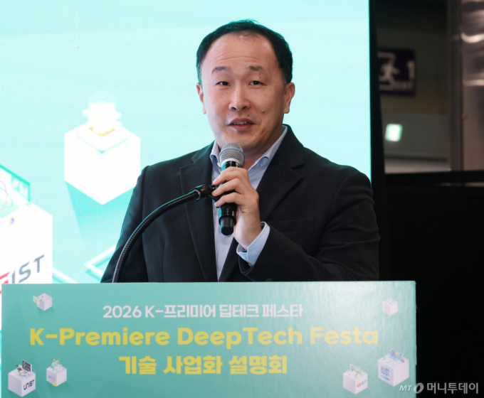
“We can boost the efficiency of power supplied to AI (artificial intelligence) semiconductors from the existing 50 percent range to a maximum of 95 percent.”
Kim Sang-hyun, a professor in the Department of Electrical Engineering at the Korea Advanced Institute of Science and Technology (KAIST), stated this while explaining the expected effects of an independently developed power supply technology for AI semiconductors at the "2026 K-Premier Deep Tech Festa" held on the afternoon of the 29th at the Plus Stage in Hall B of COEX in Gangnam-gu, Seoul.
The technology being developed by Professor Kim's team centers on vertically placing a voltage regulation device directly beneath the semiconductor chip and applying gallium nitride (GaN) material to reduce energy loss during power transmission. It is regarded as a technology that can significantly improve power supply efficiency amid the rapidly increasing power consumption of AI semiconductors.
Professor Kim received the Excellence Award for his high ratings in technological innovation and commercialization potential at the technology evaluation held that day, among the key research achievements of the four major science and technology institutes (KAIST, DGIST, UNIST, and GIST).
As the computational performance of AI semiconductors advances, their power consumption is surging. The industry has entered an era in which a single chip consumes up to 1 kilowatt (kW) of power, yet a bottleneck exists: 30% to 40% of total power is lost during transmission from external sources to the interior of the chip. Experts warn that as future power consumption increases, transmission losses could reach as high as 50%.
Conventional AI semiconductors used a method in which voltage was lowered by a voltage regulator placed next to the chip before electricity was supplied horizontally. However, this approach had a structural limitation: when supplying the same amount of power, lower voltage requires higher current, which intensifies heat generation and energy loss due to wiring resistance.
Professor Kim's team developed a technology that vertically places a voltage regulation device directly beneath the semiconductor chip to shorten the distance current must travel, in order to address this issue. The method involves delivering electricity at high voltage all the way down to just below the chip and then stepping it down to around 1 volt (V), the level the chip operates on. This minimizes the section through which a large amount of current must flow, thereby reducing power loss, according to the team.
Gallium nitride plays a central role in this process. Ultra-fast power switches required for voltage step-down lose electrical energy as heat the higher their resistance is. Gallium nitride can withstand higher voltages than conventional silicon while significantly reducing resistance, making it advantageous for minimizing power loss. The challenge of directly bonding gallium nitride devices, which require high-temperature processes, with silicon semiconductors was resolved through a proprietary heterogeneous junction process that involves manufacturing the two devices separately before joining them.
They also developed an energy storage device to ensure a stable power supply. To store large amounts of electricity in confined spaces, they secured high-density capacitor technology by applying special materials and three-dimensional structures.
The research team expects that applying this technology will improve chip power delivery efficiency from the current range of around 50 percent to between 85 and 95 percent. Related research results have been accepted multiple times at IEDM and the VLSI Symposium, major international conferences in the field of semiconductor devices.
Professor Kim said, “Until one or two years ago, there were very few places conducting similar research, but recently, related studies have been rapidly increasing in China, which has strong gallium nitride technology.” He added, “Among companies, Intel, which has long developed CPUs (central processing units) for servers, is moving the most aggressively.”
The research team is currently conducting studies to package individually developed components into a single integrated circuit. The next goal is to verify how much power supply efficiency improves at the actual circuit level by combining silicon semiconductors, gallium nitride devices, and capacitors.
Building a mass production system for commercialization is cited as a challenge. This is because the semiconductor chips responsible for computation and the voltage regulation devices must be manufactured using different processes and then combined, while foundries (semiconductor contract manufacturers) have not yet provided sufficient support for the relevant packaging process.
Professor Kim explained, “The short-term goal is to first demonstrate performance at the laboratory level and provide a technical direction that enables foundries to proceed with developing related processes.”
The company is prioritizing commercialization through technology transfer and licensing, while also considering the option of direct entrepreneurship if necessary. He stated, “When it comes to commercialization, we need to develop technologies that meet the needs of end users, which requires partners capable of joint development.” He added, “I hope this occasion will lead to the formation of partnerships with which we can discuss and deliberate on the direction of our technology.”
Microcracks in Cathode Materials Hinder All-Solid-State Batteries; “Nano-Particleization Can Solve the Problem”
Kim Un-hyuk, Professor, Department of Energy Engineering, Daegu Gyeongbuk Institute of Science and Technology (DGIST)
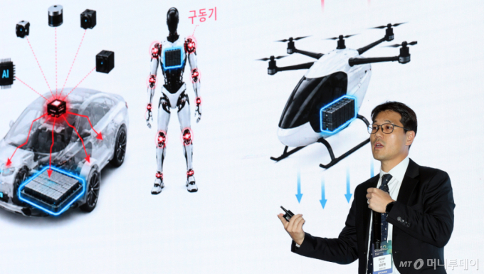
“We must fundamentally prevent the cracks that form when high-energy cathode materials fracture. Only then can we build cells using solid electrolytes and succeed in developing all-solid-state batteries.”
Professor Kim Un-hyuk of the Department of Energy Engineering at DGIST (Daegu Gyeongbuk Institute of Science and Technology) made this statement while presenting cathode material technology tailored for all-solid-state batteries at the "2026 K-Premier Deep Tech Festa" held on the 29th at COEX in Seoul Samsung-dong. The presentation explained that high-energy cathodes suffer significant performance degradation in all-solid-state batteries due to microcracks caused by particle fracture during charge and discharge cycles, and that this issue was mitigated by reducing the particles to the nanoscale.
Professor Kim explained, “Materials account for approximately 75 percent of battery costs, and cathode materials make up about 49.5 percent of that total. In other words, when purchasing an electric vehicle, roughly 25 to 26 percent of the price is effectively paid for cathode materials.”
The market trend is unfavorable for the domestic industry. Lithium iron phosphate (LFP) cathode materials made from inexpensive raw elements are expanding their market share, centered in China, and Chinese automaker BYD has taken the top spot in the electric vehicle market. Professor Kim shared his experience visiting a battery exhibition in China, stating, "I felt that if we remain complacent without lowering technology or prices, our entire industry will be taken over." He also emphasized, "Since secondary batteries are an energy security industry directly linked to national defense, such as drones, it is essential to secure domestic production technology."
Professor Kim argued that demand for high energy density batteries is actually increasing. As autonomous driving features expand, vehicle power consumption rises, while robots and drones with limited space must store large amounts of energy in small volumes. For battery backup units (BBUs) that provide instantaneous power to data centers, energy density and stability take precedence over price. Lithium iron phosphate (LFP) batteries are inexpensive and offer high thermal stability, but they have lower energy density than the nickel-cobalt-manganese (NCM)-based layered cathode materials that are the focus of domestic efforts.
Layered cathode materials offer higher capacity as nickel content increases, but their lifespan and thermal stability decline. Professor Kim compared materials with nickel content ranging from 30% to 100%, stating, "Simply adjusting the ratio of nickel, cobalt, and manganese cannot yield a material that simultaneously achieves high capacity, long lifespan, and thermal stability."
The cause of reduced lifespan is microcracks. When charging and discharging cycles are repeated, spherical cathode particles with a diameter of approximately 10 micrometers fracture, allowing the electrolyte to seep into the gaps and trigger side reactions. Professor Kim stated, "The core of this announcement is that microcracks must be eliminated." He added that fire can occur when oxygen contained in the cathode material, flammable organic liquid electrolytes, and sparks generated during a short circuit coincide. "Because oxygen is supplied from the cathode material, the fire cannot be extinguished with water and continues to burn until it is completely consumed," Professor Kim explained. "To fundamentally prevent fires, all-solid-state batteries that replace the electrolyte with a solid are necessary."
The commercialization target for all-solid-state batteries continues to be postponed. While liquid electrolytes effectively coat cathode materials, solid electrolytes are prone to interface delamination where two solids come into contact. Once an interface separates due to microcracks, it cannot be restored. In practice, using high-energy cathode materials in conjunction with solid electrolytes significantly reduces both capacity and lifespan.
Professor Kim's research team mitigated the stress that causes cracking by manufacturing cathode material particles at the nanoscale. The developed material retained more than 90% of its initial capacity after 300 charge-discharge cycles and demonstrated superior performance compared to commercial materials in high-speed charge-discharge scenarios requiring instantaneous high output, such as drone takeoffs and landings. When electrodes that had completed charge-discharge cycles were cut and examined under an electron microscope, the interface with the solid electrolyte was fractured in the commercial material, whereas the structure of the developed material remained intact.
He also highlighted the advantages in terms of commercialization. Professor Kim explained, "By introducing just one dopant element, existing equipment can be used as is." He added, "Controlling particle morphology could send shockwaves through the all-solid-state battery market," and noted, "Although it will take time to reach commercialization, we will make efforts in various areas, including patents and technology transfer."
Hot and bending AI semiconductors... Replacing them with specialty glass to create a "highway of light"
Kim Bok-hyun, Senior Researcher at the Advanced Photon Technology Research Institute, Gwangju Institute of Science and Technology (GIST)
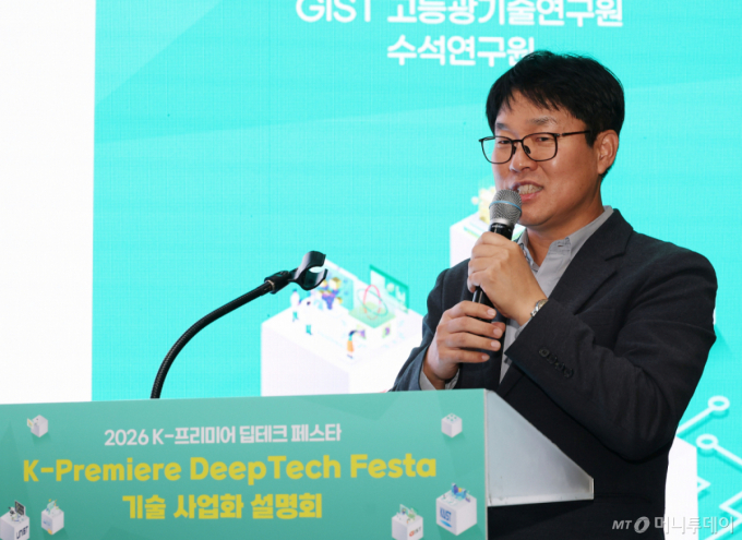
"We developed a glass material with a significantly lower dielectric constant than existing materials and a dielectric loss at one-third the level. This can also be combined with technology that uses lasers to create three-dimensional (3D) optical waveguides, enabling electrical signals to be transmitted as light."
Kim Bok-hyun, a senior researcher at the Gwangju Institute of Science and Technology (GIST) Advanced Photonics Research Institute, stated this on the 29th at the "2026 K-Premier Deep Tech Festa" held at COEX in Seoul Samsung-dong. He said, "The core differentiator is the combination of materials technology and photonics (a technology that transmits data using light)."
Researcher Kim presented on the topic of "Low-Dielectric Glass Materials and Optical Interconnect Technology for Semiconductor Glass Substrates" that day. The technology connects glass materials with semiconductor packaging and photonics to reduce signal loss and heat generation in AI semiconductors, while creating light-conduction pathways within the glass to transmit data rapidly.
The K-Premier Deep Tech Festa is a technology commercialization event that expanded and reorganized the "Tech Market," which was first held in 2024. It was co-hosted by the Ministry of Science and ICT, the four major science and technology institutes—Korea Advanced Institute of Science and Technology (KAIST), GIST, DGIST (Daegu Gyeongbuk Institute of Science and Technology), and UNIST (Ulsan National Institute of Science and Technology)—and Money Today’s Unicorn Factory.
The four major science and technology research institutes each presented two promising technologies for commercialization, totaling eight projects. Researchers directly explained the development purpose and core functions of their technologies, as well as their differentiation from existing technologies and industrial applicability. A consultation area was also set up in front of the event venue, where companies considering technology transfer and commercialization held individual consultations with the researchers.
AI (artificial intelligence) semiconductors combine multiple compute chips and high-bandwidth memory (HBM) within a single package. As the amount of data to be processed increases, the size and power consumption of semiconductor packages are also growing.
The issue lies in the substrate that supports the chip. Existing semiconductor packages primarily use organic substrates made by combining polymers and glass fiber. Because organic materials have a higher coefficient of thermal expansion than glass, they can develop “warpage,” or bending of the substrate, as temperatures rise.
Organic substrates have a relatively rougher surface than glass, which limits their ability to form fine wiring. As data transmission frequencies increase, the problem of signal attenuation on the substrate and the conversion of part of the electrical energy into heat also becomes more severe.
Researcher Kim stated, "High-performance AI semiconductors consume large amounts of power and their package areas continue to expand," adding, "Glass substrates are advantageous for reducing deformation caused by thermal expansion and for realizing high-density wiring and larger surface areas."
Researcher Kim's team designed the glass composition and internal structure from the outset to meet the requirements of high-performance semiconductor packaging. The team explained that by adjusting the composition of aluminoborosilicate glass, they reduced the dielectric constant and dielectric loss, which affect high-frequency signal loss and heat generation.
He explained, “As increasing the frequency is an inevitable trend, it is necessary to lower the dielectric constant and dielectric loss of the material,” adding that “the glass material developed by the research team reduced the dielectric loss to about one-third of that of some materials currently in use.”
The improvements were not limited to electrical performance. The research team also modified the glass composition to allow thermal expansion characteristics to be adjusted according to the intended application. Thermal stability and mechanical properties were also taken into account to prevent easy deformation during high-temperature processes.
Researcher Kim stated, "Simply lowering the dielectric constant does not make a material suitable as a semiconductor substrate." He added, "It must possess a balanced combination of signal transmission performance, thermal expansion, strength, and processability, while also withstanding actual semiconductor manufacturing processes."
The research team has secured process technologies spanning the entire production line, from glass composition and melting to bubble removal, forming, and fiber spinning. As the industry's technological direction shifted from reinforcing organic substrates with glass fibers to replacing the core of the substrate entirely with glass, the scope of the research was expanded to include glass substrate materials.
Another competitive advantage of the research team is its technology for creating "optical waveguides," which are pathways through which light travels within a glass substrate. Researcher Kim stated, "Currently, data between chips primarily moves in the form of electrical signals along copper wiring. As transmission volume and distance increase, signal loss and heat generation in the copper wiring become more severe."
The research team uses femtosecond lasers to form optical waveguides and microstructures on glass substrates. Femtosecond lasers concentrate energy over an extremely short duration, allowing for precise processing of the interior of the glass while minimizing heat transfer to the surrounding area.
He stated, "Optical interconnects, which convert electrical signals into optical signals in sections where high-speed data is transmitted, are gaining attention as a next-generation technology." He added, "By forming an optical waveguide inside the glass with a refractive index different from its surroundings, light travels along a predetermined path."
Another advantage is the ability to create a variety of three-dimensional structures, including straight lines, diagonal lines, and spirals. The explanation notes that even if the positions of optical fibers, substrates, and semiconductor chips differ from one another, the path of light can be designed in three dimensions.
Meanwhile, Researcher Kim received an encouragement award at a ceremony held to celebrate the achievements of each research team and encourage future challenges. The judging was conducted by the Korea Technology Commercialization Promotion Agency (COMPA) and the Korea Science and Engineering Foundation (KISTI), based on criteria such as technological maturity, market linkage potential, and industrial impact.
Interest from corporate officials in Researcher Kim's low-dielectric glass material and optical interconnect technology continued at the technical consultation sessions set up in front of the venue. Researcher Kim held individual consultations with them regarding technology transfer, joint research, and commercialization possibilities.
Researcher Kim emphasized, “By securing both material technology and optical waveguide technology, we can simultaneously solve the power and data transmission issues of AI semiconductors,” adding, “We will expand cooperation with demand-side companies to apply our research results to actual semiconductor packages.”
“Breaking the Limits of Silicon Semiconductors”... Innovative Synthesis Technology Solves the Challenges of “2D Semiconductors”
Professor Im Hyun-seop, Department of Chemistry, Gwangju Institute of Science and Technology (GIST)
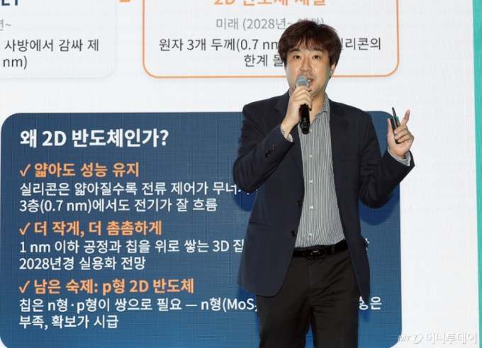
"Current two-dimensional (2D) semiconductor synthesis technology is similar to a 'restaurant's secret recipe.' While specific research groups or equipment may produce high-quality samples, attempts to replicate the process elsewhere often fail. The role of our laboratory is to identify and control the elements necessary to franchise this restaurant recipe."
Professor Im Hyun-seop of the Department of Chemistry at GIST (Gwangju Institute of Science and Technology) stated, "If we translate the 'hand feel' of the synthesis process into numbers and principles, anyone will be able to synthesize 2D semiconductor materials with high reproducibility." He made these remarks on the 29th at the "2026 K-Premier Deep Tech Festa" held at COEX in Seoul Samsung-dong.
Professor Im delivered a presentation on the topic of “High-Quality Two-Dimensional Semiconductor Thin Film Synthesis Technology” that day. The research elucidates the synthesis principles of two-dimensional semiconductor materials by bridging chemistry, semiconductor engineering, and fundamental science, and develops these into processes that can be utilized industrially.
The semiconductor industry has evolved by shrinking transistors to integrate more devices onto a single chip. However, as semiconductor processes have scaled down to below the 2nd-nanometer (nm) level, the core challenge has shifted from simply reducing size to determining what material will be used for the transistor channel.
A material gaining attention as an alternative is 2D semiconductors, which are only a few atomic layers thick. Representative examples include transition metal dichalcogenide (TMD) materials such as molybdenum disulfide (MoS₂), tungsten disulfide (WS₂), and tungsten diselenide (WSe₂).
Professor Im stated, "As we approach the physical limits of continuously increasing integration using silicon alone, changes in the materials used for channels will be necessary in the future," adding, "Major semiconductor companies such as TSMC, Samsung Electronics, and Intel are also conducting research on 2D semiconductor materials, including MoS₂."
To apply two-dimensional semiconductors in industrial settings, high-quality thin films must be uniformly produced across entire large wafers. In particular, a key challenge is reducing "grain boundaries," which form where crystals grown in different directions meet.
When a thin film grows, if multiple crystal nuclei form simultaneously at various points, each crystal can grow in a different direction. At the boundaries where these crystals meet, electrons are scattered, impeding their movement. This leads to reduced device performance and causes variations in characteristics depending on the location on the wafer.
Professor Im’s research team focused on “epitaxial growth,” a method in which a thin film is grown along the crystal structure of the substrate to align the crystal orientation. However, because the symmetry of the sapphire substrate differs from that of the MoS₂ thin film, there was an issue in which crystals oriented in two directions flipped 180 degrees could grow simultaneously.
The research team identified that by controlling the atomic arrangement and edge structure on the surface of a sapphire substrate, MoS₂ crystals can be induced to grow in a specific direction. A notable feature of this work is that it elucidated at the atomic level how the substrate surface determines the crystal orientation, rather than simply identifying successful synthesis conditions.
Professor Im compared the difficulty of synthesizing solid-state materials to grilling a steak. He explained that even when using the same cut of meat and recipe, the outcome can vary depending on whether one places the meat on the grill before starting the timer or starts the timer before placing the meat on the grill.
The same applies to 2D semiconductor synthesis. Subtle differences in precursor supply volume, substrate surface condition, reaction temperature and pressure, gas flow, and process sequence affect the thickness of the thin film, crystal orientation, and defect density.
In particular, 2D semiconductors are synthesized at high temperatures of approximately 500 degrees Celsius, even under conservative estimates. As the temperature rises, the likelihood of unexpected chemical reactions increases, making it difficult to selectively grow only the desired material.
The research team utilized inorganic molecular precursors, which can be supplied precisely in a gaseous state, instead of conventional solid raw materials. While it is difficult to precisely control how much of a solid raw material actually vaporizes during the heating process and reaches the substrate, the amount of molecular precursor fed into the system can be finely adjusted using flow controllers and valves.
Professor Im stated, "We have developed technology to synthesize high-quality 2D semiconductor thin films at the level of 2-inch wafers," emphasizing that they have secured techniques for controlling crystal size and defects by adjusting factors such as substrate surface conditions, precursor supply, and gas flow.
Meanwhile, the K-Premier Deep Tech Festa is a technology commercialization event that expanded and reorganized "Tech Market," which was first held in 2024. It was co-hosted by the Ministry of Science and ICT, the four major science and technology institutes—Korea Advanced Institute of Science and Technology (KAIST), GIST, DGIST (Daegu Gyeongbuk Institute of Science and Technology), and UNIST (Ulsan National Institute of Science and Technology)—and Money Today’s Unicorn Factory.
The four major science and technology research institutes each presented two promising technologies for commercialization, totaling eight projects. Researchers directly explained the purpose of development, core functions, differentiation from existing technologies, and industrial applicability of each technology. A consultation area was also set up in front of the event venue, where companies considering technology transfer and commercialization held individual consultations with the researchers.
Professor Im received the Encouragement Award at a ceremony held to celebrate the achievements of each research team and encourage future challenges. The judging was conducted by the Korea Technology Commercialization Promotion Agency (COMPA) and the Korea Science and Engineering Foundation (KISTI), based on criteria such as technological maturity, market linkage potential, and industrial impact.
[Money Today Startup Media Platform Unicorn Factory]

 in FUTURE


