

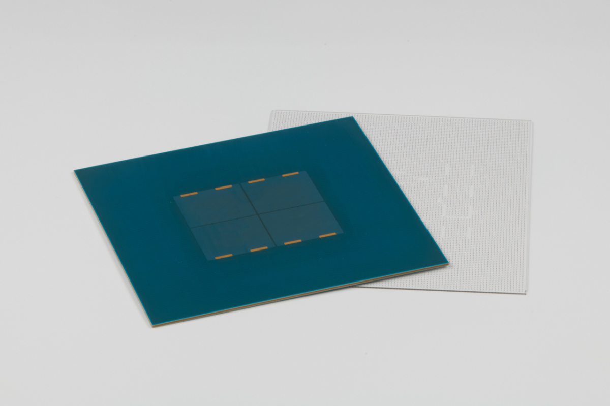
Samsung Electro-Mechanics is verifying the reliability of the packaging stage by bonding customer chips onto large glass substrates, which are gaining attention as next-generation semiconductor substrates. The company has completed verification of the glass substrates themselves after providing samples to customers. Commercialization of glass substrates is accelerating due to the scaling up of AI (artificial intelligence) accelerators and increased infrastructure investment.
According to electronics industry sources on the 6th, Samsung Electro-Mechanics has completed reliability verification for its glass substrates under development and has moved on to verifying the packaging stage where actual semiconductors are assembled. The company is currently also conducting development collaborations with multiple major global corporations. The goal is to start operations of the glass substrate production line by the end of 2027.
The glass substrates under development by Samsung Electro-Mechanics are reported to be 100mm x 100mm in size. Considering that the package substrate for NVIDIA’s Blackwell GPU (graphics processing unit) is approximately 81.5mm x 74.8mm, the area is more than 60% larger. More than 20 circuit layers, which transmit power and various electrical signals, are implemented, and it also incorporates more than 80 IPDs (integrated passive devices), which handle tasks such as stabilizing power supply.
The scaling up of AI accelerators is the background for why glass substrates are gaining attention. As multiple chips, including GPUs and HBM (high-bandwidth memory), are integrated into a single package, substrates are also rapidly increasing in size. Existing organic material substraces become difficult to maintain precision in fine circuits while suppressing warping as their size increases.
Glass substrates apply glass to the core material, reducing warping and maintaining high flatness and dimensional stability even over large areas. They can improve signal and power characteristics while reducing the number of circuit layers, making them considered a next-generation substrate for large-scale, highly integrated AI semiconductors.
The industry expects demand for large package substrates with one side measuring around 100mm to fully materialize starting from NVIDIA’s Rubin generation. It is reported that NVIDIA has requested major global substrate manufacturers to commercialize glass substrates within two years. China’s largest display manufacturer, BOE, is also moving into glass substrate development and investment, expanding the competition for market leadership.
Samsung Electro-Mechanics is expanding its investment in package substrates for AI servers. Recently, it decided on an expansion investment of 427 billion won to increase production capacity for FCBGA (Flip Chip-Ball Grid Array) at its Sejong plant. The company also plans to invest 251 billion won in expanding its package substrate factory in Vietnam.
To expand production capacity, it ordered approximately 24.5 billion won worth of "Micro Saw and Vision Placement (MSVP)" equipment from Hanmi Semiconductor. MSVP is a back-end process equipment that performs precision cutting, inspection, and placement processes, used for printed circuit boards and glass substrates. Since Hanmi Semiconductor experienced past patent disputes with Semes, a subsidiary of Samsung Electronics, large-scale orders from Samsung affiliates have been effectively suspended since the early 2010s.
The expansion of AI infrastructure is also leading to increased orders for MLCCs (multilayer ceramic capacitors), a core business of Samsung Electro-Mechanics. On this day, Samsung Electro-Mechanics signed a long-term supply contract worth 290 billion won with a major global corporation for MLCCs for AI servers. This is the sixth long-term supply contract this year, bringing the cumulative contract value to approximately 390 billion won.

 in INDUSTRY
