

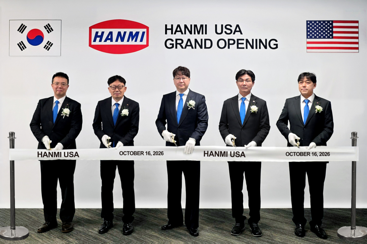
Hanmi Semiconductor said Monday that it held an opening ceremony for its Hanmi USA office in San Jose, California, U.S., on the 16th (local time). Key executives, including Hanmi Semiconductor Chairman Kwak Dong-shin, attended the event.
The company explained that the establishment of Hanmi USA holds deep significance as it realizes the entrepreneurial spirit embedded in the 'Hanmi' name after 46 years since its founding. The name 'Hanmi' reflects the late founder Kwak No-gwon's intention to serve as a bridge connecting the semiconductor industries of Korea and the United States.
Founder Kwak No-gwon worked at Motorola in the U.S. for 14 years, starting in 1967. He subsequently established Hanmi Semiconductor in Korea in 1980 with support from Motorola. Having grown into a global advanced semiconductor packaging equipment company, Hanmi Semiconductor has now realized the founder's vision on local soil through the establishment of Hanmi USA.
Following the establishment of Hanmi Taiwan, Hanmi China, and Hanmi Singapore, Hanmi Semiconductor has further strengthened its global supply chain with the launch of Hanmi USA. Based in San Jose, Silicon Valley—a hub for global semiconductor companies and big tech firms—Hanmi USA will serve as an integrated operational base and enhance technical support for local U.S. customers.
In particular, the company plans to deploy skilled engineers locally and proactively provide intensive technical support in line with the operational schedules of new factories being built by global semiconductor companies in the United States.
Kwak Dong-sin, chairman of Hanmi Semiconductor, said, "The U.S. is a crucial market leading the world's AI industry and advanced semiconductor technology." He added, "Hanmi USA will provide intensive technical support to local U.S. customers and expand cooperation with global semiconductor companies to further strengthen our competitiveness in the global market."

 in INDUSTRY
