

'Dream material' applied like ink… Semiconductor for 6G and space communications crafted in a flash
Kim Myung-soo, Professor, Department of Electrical and Electronic Engineering, Ulsan National Institute of Science and Technology (UNIST)
Development of solution process technology for manufacturing semiconductor devices using two-dimensional materials
Fabrication of high-performance 'RF switches'… Commercialization potential in defense sector and beyond
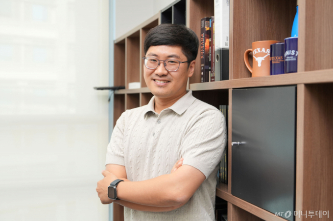
Two-dimensional (2D) materials, such as graphene or molybdenum disulfide (MoS₂), which consist of layers only a few atoms thick, are considered next-generation materials capable of overcoming the miniaturization limits of existing silicon-based semiconductors. While research labs and companies at home and abroad are racing to study them, commercialized cases remain rare due to the difficulty in handling these materials, such as synthesizing them in large sizes and bonding them.
The team led by Kim Myung-soo, Professor of Electrical and Electronic Engineering at Ulsan National Institute of Science and Technology (UNIST), solved this problem with an 'ink' approach. This method involves creating 2D materials into ink and applying it to a substrate via a 'solution process' to manufacture semiconductor devices. Using this technology, the team created RF switches that operate in the ultra-high frequency band. These are communication chips used in high-frequency environments such as 6G (6th-generation mobile communications) and satellite communications.
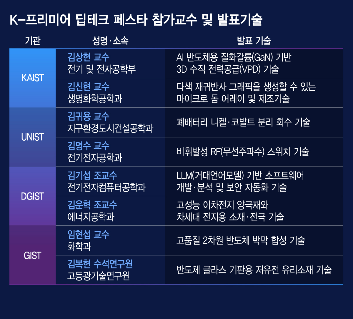
The research team led by Professor Kim will unveil this technology at the '2026 K-Premier Deep Tech Festa' (Registration: https://url.kr/kpy365), to be held on the 29th at Seoul COEX. The team plans to explain the significance of the solution process and the application value of the RF switches made with this technology in national strategic industries such as 6G, satellite communications, radar, and defense.
There are primarily two methods for manufacturing semiconductor devices using 2D materials. The first is the exfoliation method, which peels off 2D materials layer by layer. While quality is excellent, the peeled flakes are too small to be precisely placed on wafers. The second is the transfer method, where materials are synthesized on a wafer using techniques such as chemical vapor deposition and then transferred to another substrate. This approach also faces hurdles in synthesizing and transferring the material, as well as maintaining uniform quality of the transferred film.
Professor Kim's team chose a different approach: dissolving the material in a solution to create ink, which is then coated onto a substrate. Professor Kim stated, "Small flakes overlap irregularly to cover the surface without gaps," adding, "We achieved the desired device characteristics simply by applying ink, without the need to peel and attach pieces individually or scale them up significantly."
The research team fabricated an RF switch using this technology. This component connects or disconnects the path of high-frequency signals exchanged via antennas in smartphones, satellites, radar, and base stations. When a molybdenum disulfide film made from ink is placed between metal electrodes and voltage is applied, copper ions emitted from the copper electrode create a conductive pathway, turning the switch on. A characteristic feature is that once formed, this pathway remains even when power is turned off ('non-volatile'), meaning no standby power is consumed.
According to the research team, this RF switch demonstrated performance passing approximately 98% of input signals at the 67th GHz ultra-high frequency used for high-speed communications. It also showed higher durability than existing exfoliation methods (approximately 100 cycles), with no performance degradation even after more than 2,000 repeated operations.
The team identified defense and space sectors as key demand areas for the developed RF switch. Professor Kim noted, "It operates well at very low or high temperatures, offering potential in extreme environments such as space," and added, "Most components for defense-grade applications are imported from overseas; producing them domestically would benefit domestic companies."
Professor Kim stated, "The significance of this research lies in making 2D materials easier to use," adding, "It allows semiconductor devices to be made more easily and quickly with stable performance." He further elaborated, "The RF switch, which demonstrated this potential, offers multiple advantages including performance, cost, operation across a wide frequency band, and power savings."
However, Professor Kim drew a line, stating that 2D materials cannot immediately replace silicon using solution process technology. He said, "It should be viewed as an effort to complement the shortcomings of existing technologies with new materials and approaches," adding, "As the technology is further refined, its industrial applicability will expand."
Extracting only desired metals from spent batteries… New technology reduces wastewater treatment and cost burdens
Kim Ki-yong, Professor, Department of Earth Environment and Urban Construction Seol Gong-hak-gwa (Prof.), Ulsan National Institute of Science and Technology (UNIST)
Development of technology to extract only desired metals via electrodeposition instead of chemical substances
"Extract purity 99.9%, recovery rate 95%… Reduces wastewater treatment and cost burdens"
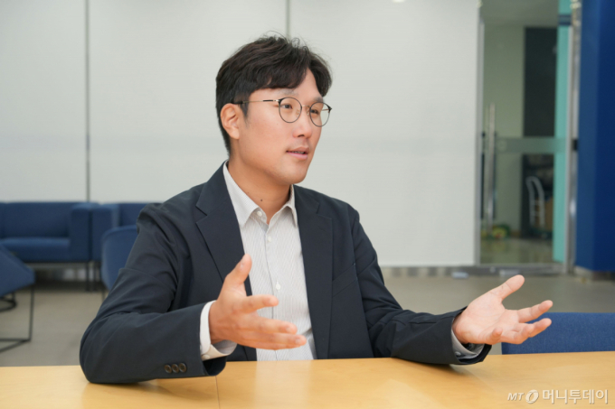
Spent batteries are called 'urban mines' because they contain large amounts of valuable metals such as nickel and cobalt. However, extracting these requires powerful chemical substances. Since various metals are mixed together, a purification process is necessary to extract the desired material. As a result, instead of just obtaining metal, large volumes of wastewater containing chemicals are generated.
The team led by Kim Ki-yong, Professor of Earth Environment and Urban Construction Seol Gong-hak-gwa (Prof.) at Ulsan National Institute of Science and Technology (UNIST), developed an extraction technology that minimizes wastewater generation in this process. Instead of using large amounts of chemicals, this electrical recovery technology sends electricity to sequentially select nickel and cobalt. The purity of the extract is over 99.9%, with a recovery rate reaching 95%.
At the '2026 K-Premier Deep Tech Festa' (Registration: https://url.kr/kpy365) to be held on the 29th at Seoul COEX, Professor Kim's research team will unveil this spent battery nickel and cobalt separation and recovery technology. The team plans to introduce effects from an ESG (Environment, Social, and Governance) management perspective and cost-saving benefits when utilized by companies.
According to Professor Kim, recycling spent batteries typically involves first disassembling and crushing the batteries into 'black powder' and dissolving them in a strong acidic solution. Subsequently, 'solvent extraction' is performed by adding chemicals (organic solvents) to the acidic solution containing the dissolved black powder to sequentially select the desired metals.
Professor Kim's team's technology bypasses this solvent extraction step. Professor Kim stated, "Instead of solvent extraction, we send electricity through the mixed metal solution (electrodeposition) to extract the desired metal." This method utilizes the fact that each metal has a different voltage at which it turns solid, allowing specific metals to be selected by adjusting the voltage.
Professor Kim's team was not the first to develop the electrodeposition method. However, extraction was difficult because nickel and cobalt react at similar voltages. The team solved this problem by using 'deep eutectic solvents (DES)' that alter the ionic properties of nickel and cobalt. Professor Kim explained, "Applying changes in metal ionic properties to metal recovery is the significance of this technology."
Professor Kim emphasized, "By omitting solvent extraction, we can reduce not only the burden of wastewater treatment but also process costs." While electrodeposition requires raising the temperature of liquefied black powder and using additional electricity, he explained that these costs are small compared to the savings. Deep eutectic solvents can be recycled multiple times, so additional wastewater generation is minimal. Professor Kim plans to further improve this aspect by enhancing reactors and increasing the number of solvent reuse cycles.
The scale of the domestic spent battery recycling industry is a hurdle to overcome. This is because electric vehicles scrapped domestically are being exported to Southeast Asia and other regions where process, labor, and wastewater treatment costs are lower. However, if technologies that reduce recovery costs spread, incentives to process spent batteries domestically rather than sending them overseas may also grow.
Professor Kim viewed spent battery recycling companies as the primary demand source for this technology. Theoretically, the scope of application is broader. Professor Kim stated, "The same principle allows metal recovery for companies discharging wastewater mixed with nickel and cobalt, or companies refining nickel ore and concentrate," adding, "Fields such as metal refining and wastewater treatment can also become demand sources for the technology."
<Registration for 'K-Premier Deep Tech Festa (Technology Transfer and Commercialization)'>
- Date: October 29, 2026 (Thu), 1:00 PM
- Location: Hall B PLUS STAGE, COEX, Samsung-dong, Seoul
- Target Participants: Companies considering technology transfer, joint research, or new businesses; family companies of government-funded research institutes; investment firms
- Participation Fee: Free (Pre-registration required)
- Hosts: Ministry of Science and ICT, KAIST, GIST, DGIST, UNIST, MoneyToday Unicorn Factory
- Sponsors: Korea Institute of Science and Technology Information (KISTI), Commercialization Promotion Agency for R&D Outcomes (COMPA)
- Application: https://url.kr/kpy365
[MoneyToday Startup Media Platform Unicorn Factory]

 in FUTURE


