

Samsung Electronics is expanding its advanced process production capacity in foundry (semiconductor contract manufacturing) driven by growth in the HBM (high-bandwidth memory) market. With surging demand for 6th-generation HBM (HBM4) base dies, the company is moving to full operation of its 4nm (㎚·one-billionth of a meter) process and is considering capacity expansion. There are also discussions about potential investment in new 2nm production lines to prepare for HBM5 (8th generation).
According to the electronics industry on the 21st, Samsung Electronics is reviewing capacity expansion for its foundry 4nm process to meet growing demand for HBM4 base dies. Samsung Electronics' HBM4 consists of a core die using 10nm-class 6th-generation (1c) DRAM and a logic semiconductor base die produced via the 4nm process.
The base die serves as the connection layer at the bottom of HBM, enabling rapid data exchange between GPU (graphics processing unit) and AI (artificial intelligence) accelerators. As HBM's operating speed increases and capacity grows, the base die's data processing performance and power efficiency become increasingly critical. Starting with HBM4, advanced foundry processes have been applied to the base die, establishing it as a key factor in enhancing HBM's performance and power efficiency.
Unlike SK Hynix, which utilizes TSMC's 12nm process for its HBM4 base dies, Samsung Electronics has adopted its own 4nm process to boost performance and power efficiency. Samsung Foundry's 4nm 4th-generation process, having been sufficiently validated in terms of performance and yield during the fourth year of Yangsan operations, played a significant role in the early adoption of HBM4.
Samsung Electronics' 4nm production lines are already operating at full capacity. In addition to expanding HBM4 production, NVIDIA's AI inference semiconductor "Groq 3 LPU (language processing unit)" is also being manufactured using Samsung Foundry's 4nm process. With surging demand, Samsung Electronics recently raised prices for new 4nm orders. Reports indicate that prices for HBM4 base dies have also been increased.
Especially, with the anticipated expansion of NVIDIA's next-generation AI platform "Vera Rubin" in the second half of the year, HBM4 demand is expected to surge significantly. Samsung Electronics forecasts that HBM4 revenue in the third quarter will more than triple compared to the previous quarter. It also projects that HBM4 will account for over 60% of total HBM revenue for the entire second half of the year.
To respond to HBM demand, Samsung Electronics plans to allocate most of the additional expansion capacity at its P4 (Factory 4) in Pyeongtaek, Gyeonggi Province, to production of 1c DRAM for HBM. It is also reported that Samsung Foundry has already allocated more than half of its current 4nm production capacity to HBM4 base die manufacturing.
Furthermore, the 4nm base die will also be applied to HBM4E, the 7th-generation HBM. Samsung Electronics became the first in the industry to supply HBM4E samples to customers last May and is currently discussing detailed specifications. Industry observers believe that once HBM4 and HBM4E become mainstream products, current 4nm production capacity alone will be insufficient to meet demand, necessitating expansion of base die production capabilities.
Samsung Electronics is also considering the construction of new 2nm production lines to prepare for HBM5. The HBM5 base die will utilize a 2nm process with GAA (gate-all-around) structure and aim to increase TSV (through-silicon via) integration density, targeting over 50% improvement in operating speed compared to HBM4E. This reflects a structural trend where HBM generation transitions drive demand for advanced foundry processes and new investments.
Samsung Electronics began its first-generation 2nm process at Yangsan in the second half of last year and has now started production of products based on the improved 2nd-generation 2nm process with enhanced yield and performance in the second half of this year. Its customer base is expanding to include mobile APs (application processors) and Tesla, among others. The strategy aims to solidify technological leadership by proactively adopting the 2nm process for HBM5.
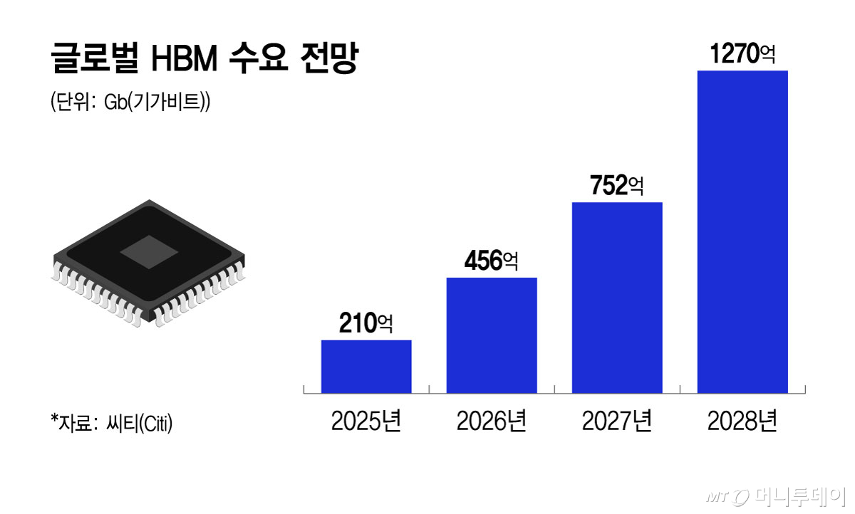
The growth trajectory of the HBM market is also steep. Citigroup predicts that global HBM bit demand will reach 75.2 billion Gb (gigabits) next year, a 62% increase from this year, and expand to 127 billion Gb by 2028. Conversely, next year's supply is expected to be only 59.4 billion Gb, leaving a shortfall of approximately 21% against demand.
Samsung Electronics' HBM supply expansion speed is also expected to accelerate. Citigroup forecasts that Samsung Electronics' HBM supply will increase by 2.3 times compared to this year next year, with its market share rising from 30% this year to 42% next year, securing the top position.
An industry insider stated, "The base die played a major role in Samsung Electronics' HBM4 success," adding, "The foundry business unit is expected to achieve profitability soon."

 in INDUSTRY
