

Two-dimensional materials, such as graphene or molybdenum disulfide (MoS₂), which consist of thin layers only a few atoms thick, are considered next-generation materials capable of breaking through the miniaturization limits of existing silicon-based semiconductors. While research labs and companies at home and abroad are racing to study them, commercialized cases remain rare. This is because handling these materials—such as synthesizing them in large sizes and bonding them—is difficult.
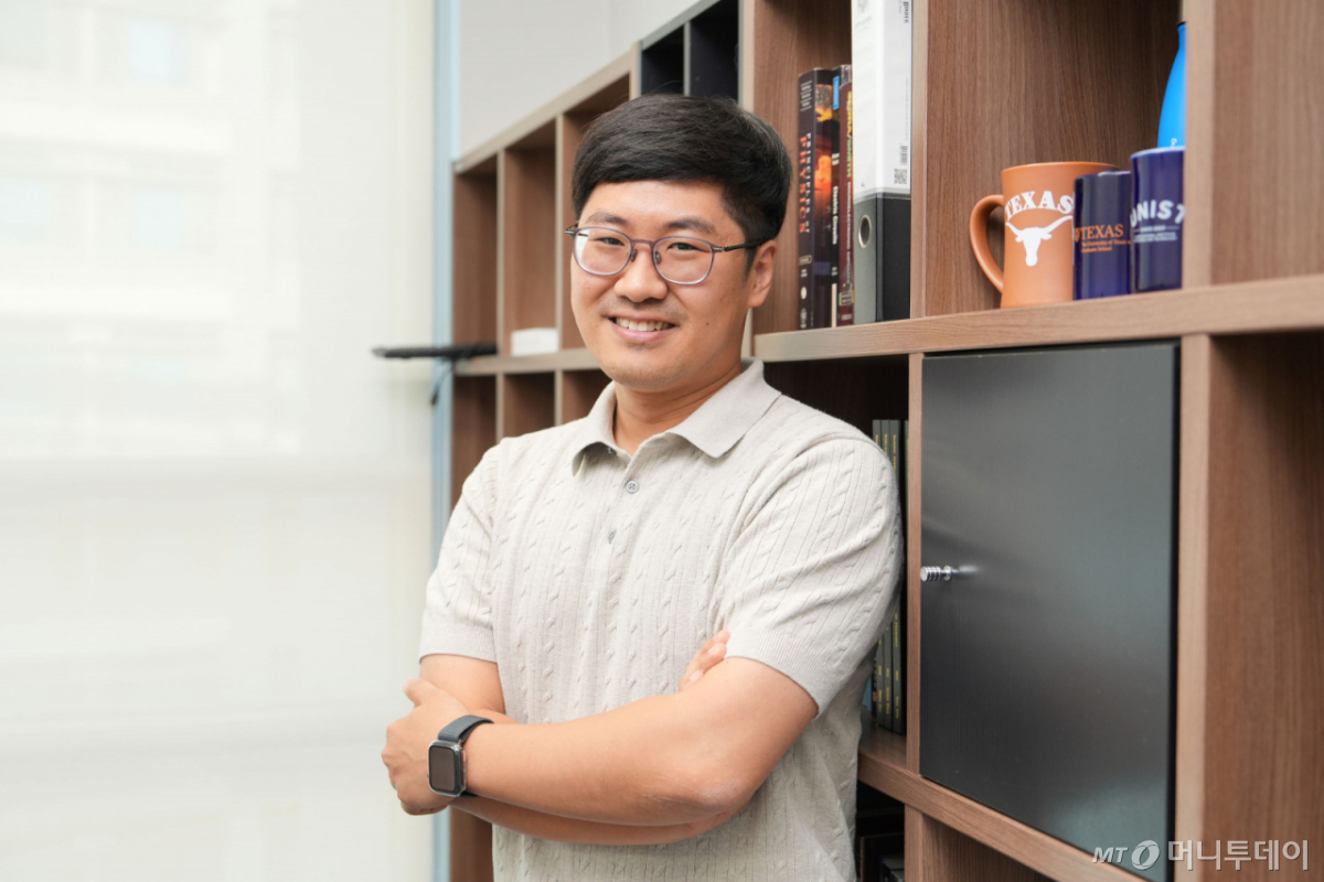
The team led by Professor Kim Myung-soo of the Department of Electrical and Electronic Engineering at Ulsan National Institute of Science and Technology (UNIST) solved this problem using an "ink" approach. It is a method of manufacturing semiconductor devices through a "solution process," where two-dimensional materials are turned into ink and applied to a substrate. Using this technology, Professor Kim's team created RF switches that operate in the ultra-high frequency band. These are communication chips used in high-frequency environments such as 6G (6th-generation mobile communications) and satellite communications.
At the '2026 K-Premier Deep Tech Festa ' (Registration: https://url.kr/kpy365 ) to be held on the 29th at COEX in Seoul, Professor Kim's research team will unveil this technology. They plan to explain the significance of the solution process and the application value of the RF switches made with this technology in national strategic industries such as 6G, satellite communications, radar, and defense.
Semiconductors from ink… "Solution process" that surpasses limits
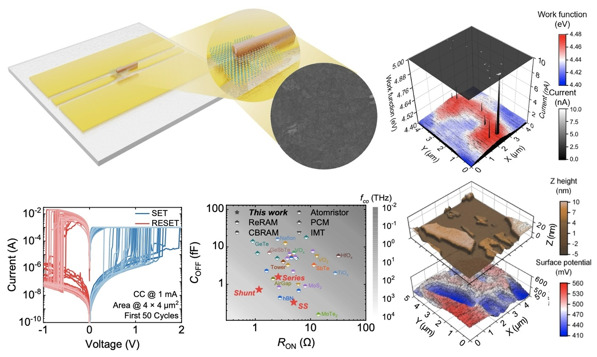
There are mainly two methods for manufacturing semiconductor devices using two-dimensional materials. The first is the exfoliation method, which peels off two-dimensional materials layer by layer. While quality is excellent, the peeled flakes are too small to be precisely placed on a wafer. The second is the transfer method, where materials are synthesized on a wafer using techniques such as chemical vapor deposition and then transferred to another substrate. This method also faces hurdles in synthesizing and moving the material, as well as maintaining uniform quality of the transferred film.
Professor Kim's team chose a different approach: dissolving the material in a solution to create ink, then coating it onto a substrate. Professor Kim stated, "Small flakes overlap irregularly to cover the surface without gaps," adding, "Without needing to peel and attach them one by one or grow them large, we extracted the desired device characteristics simply by applying the ink."
The research team fabricated an RF switch using this technology. It is a component that connects or disconnects the path of high-frequency signals exchanged via antennas in smartphones, satellites, radar, and base stations. When a molybdenum disulfide film made from ink is placed between metal electrodes and voltage is applied, copper ions emitted from the copper electrode create a conductive pathway, turning the switch on. The pathway formed remains even after power is turned off, making it "non-volatile," which means it does not consume standby power.
According to the research team, this RF switch demonstrated performance passing approximately 98% of input signals at the 67th GHz ultra-high frequency used for high-speed communications. It also showed higher durability than existing exfoliation methods (approximately 100 cycles), with no performance degradation even after more than 2,000 repeated operations.
"Zero standby power" RF switch… Increased utility in 6G and satellite communications
The defense and space sectors were cited as demand areas for the developed RF switch. Professor Kim noted, "It operates well at very low or high temperatures, showing potential in extreme environments like space," and added, "Most components for military-grade applications are imported from overseas, so being able to produce them domestically would benefit domestic companies."
Professor Kim said, "The significance of this research lies in making two-dimensional materials easier to use," stating, "It allows semiconductor devices to be made more easily and quickly, with stable performance." He further elaborated, "The RF switch that demonstrated this potential has multiple advantages, including performance, cost, operation across a wide frequency band, and power savings."
However, Professor Kim drew a line, stating that two-dimensional materials cannot immediately replace silicon using solution process technology. He said, "It should be viewed as an effort to complement the shortcomings of existing technologies with new materials and approaches," adding, "If the technology is further refined, its industrial applicability will increase."
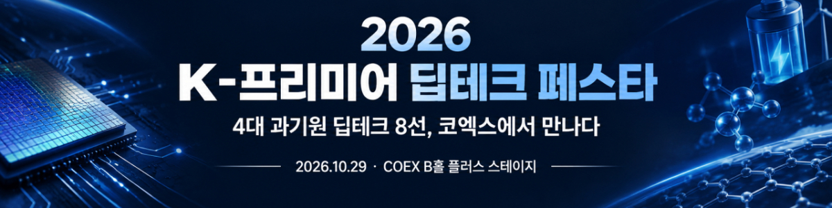
<Registration for 'K-Premier Deep Tech Festa (Technology Transfer & Commercialization)' >
- Date: October 29, 2026 (Thu), 1:00 PM
- Location: COEX Hall B PLUS STAGE, Samsung-dong, Seoul
- Target participants: Companies considering technology transfer, joint research, or new business ventures; family companies of government-funded research institutes; investment firms
- Participation fee: Free (Advance registration required)
- Hosts: Ministry of Science and ICT, KAIST, GIST, DGIST, UNIST, MoneyToday Unicorn Factory
- Sponsors: Korea Institute of Science and Technology Information (KISTI), Commercialization Promotion Agency for R&D Outcomes (COMPA)
- Application: https://url.kr/kpy365
[MoneyToday startup media platform Unicorn Factory]

 in FUTURE


