


Samsung Electronics presented zHBM, a next-generation 3D high-bandwidth memory (HBM) designed to resolve bottlenecks in the AI era, and a 10th-generation V-NAND model featuring over 400 stacked layers, marking the world's first.
Samsung Electronics announced that it participated in 'FMS (Future of Memory and Storage) 2026', held from the 4th to the 6th (local time) at the Santa Clara Convention Center in California, U.S., and unveiled for the industry its first mock-ups of zHBM and zNAND-O, next-generation 3D memory architectures.
At 'FMS 2026', Samsung Electronics showcased an exhibition booth visualizing AI cloud servers and displayed approximately 30 products centered on its memory portfolio ranging from DRAM to NAND and storage.
On the first day of the event, the morning of the 4th, Lee Jin-yeop, Vice President of the Flash Development Division, and Kim Kyung-ryun, Senior Executive of the DRAM Development Division, delivered keynote speeches on the theme 'Driving the wave of AI Revolution: 3D Innovations in Memory & Storage Architecture'. The two speakers presented a technical vision to address growing demand for high-performance computing (HPC) and AI infrastructure based on next-generation 3D memory such as zHBM and zNAND-O, aiming to maximize the performance and power efficiency of AI systems.
First, Samsung Electronics proposed zHBM as an alternative. zHBM goes one step further than the existing method of placing HBM beside AI accelerators (xPUs), by vertically stacking HBM on top of AI accelerators. By minimizing data transfer distances between AI accelerators and memory, it increases bandwidth and power efficiency while supporting ultra-fast data processing required for training and inference of large-scale AI models. The company explained that this system offers performance up to eight times higher than HBM5 (8th generation), which has not even been completed in development yet.
Furthermore, due to the shortened data transfer distance, it improves power efficiency by up to three times compared to HBM5 and reduces thermal resistance by more than half, thereby maximizing the stability and power efficiency of high-capacity, high-bandwidth systems. In addition, zHBM allows for customer-customized design. By adding customized IP (Intellectual Property—design blocks that implement specific semiconductor functions as circuits) to the interlayer located between memory and AI accelerators, product characteristics such as memory capacity expansion and accelerator performance enhancement can be optimized.
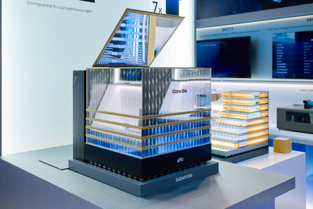
zNAND-O, a next-generation NAND product under development by Samsung Electronics, utilizes existing V-NAND vertical stacking technology combined with TSV (Through-Silicon Via) technology to create a 3D-packaged product consisting of four or eight semiconductor chips. The '-O' at the end of the product name signifies that it is optimized for on-device AI environments. Based on high space efficiency, data loading bandwidth, and fast response speeds, it supports high performance in environments requiring real-time large-scale data processing.
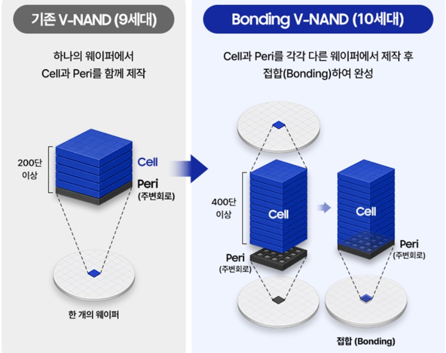
Samsung Electronics also unveiled its V10 BV-NAND with over 400 layers for the first time in the industry. BV (Bonding Vertical) is a technology that separates cells and circuits for individual manufacturing before vertically bonding them together. This demonstrates continued technological innovation since Samsung Electronics first announced V-NAND technology at the same event 13 years ago.
Through wafer bonding (vertically joining two or more wafers) and 3-stack technologies (manufacturing V-NAND cells divided into three stacks separately before connecting them vertically), the company achieved ultra-high stacking of over 400 layers, improving memory integration density by approximately 58% compared to the previous generation (V9), enabling more data to be stored in the same area.
In particular, V10 BV-NAND does not merely increase the number of stacked layers; it also improved data read/write performance and I/O (data input/output) speeds compared to the previous generation.
Additionally, at this event, Samsung Electronics exhibited a next-generation AI platform equipped with HBM4E (7th generation) and wafers, and also unveiled an HBM5 mock-up that applies a new thermal management technology called HPB (Heat Path Block) to provide higher bandwidth and capacity.
A Samsung Electronics official stated, "Samsung Electronics is the only comprehensive semiconductor (IDM) company in the world capable of providing a 'one-stop solution' covering memory, logic, foundry, and packaging." The official added, "Going forward, we plan to continue strengthening our leadership in semiconductor technology for the AI era through innovations in next-generation memory technologies and differentiated solutions encompassing memory, foundry, and advanced packaging."

 in INDUSTRY


