

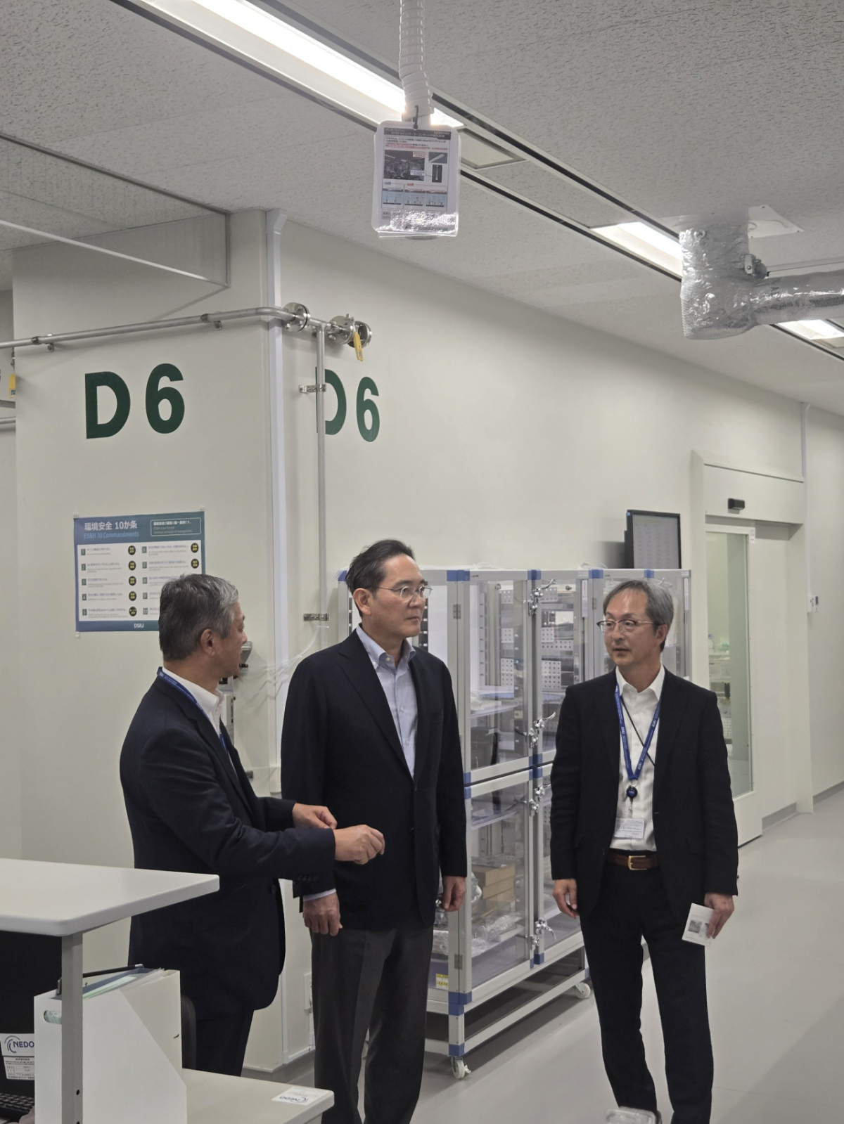
Lee Jae-yong, Chairman of Samsung Electronics, visited a semiconductor research hub in Japan to oversee development progress. The visit aimed to directly inspect packaging (post-process) technology, which is considered key to enhancing the performance of next-generation AI (artificial intelligence) semiconductors, while also emphasizing collaboration with outstanding local Japanese materials, components and equipment companies.
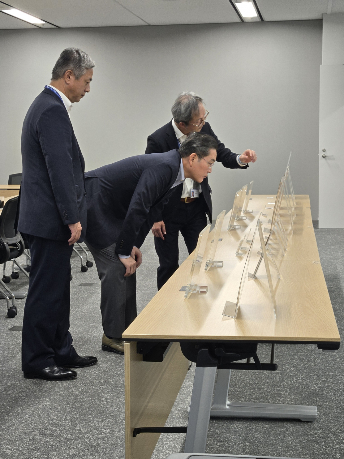
According to Samsung on the 1st, the Chairman visited "APL" (Advanced Package Lab), an advanced semiconductor packaging research hub in Yokohama, Japan, that afternoon to review research status. The Chairman discussed material and process element technology development tasks, as well as cooperation plans with the Japanese materials, components and equipment industry, together with researchers.
As Samsung Electronics' packaging research hub in Japan, which officially opened on September 8, APL received a visit from the Chairman at its site within two months. Samsung Electronics established APL in 2023 and is building a research foundation in Japan after deciding to invest 40 billion yen (approximately 350 billion won) over five years starting from 2024.
True to its name, APL develops technologies required for packaging. In AI semiconductors, packaging capability has emerged as a core competitive advantage independent of individual chip performance. This is because the technology that integrates various semiconductors, such as GPUs (graphics processing units), HBM (high-bandwidth memory), and accelerator chips, into a single package significantly impacts the bandwidth, power efficiency, and heat dissipation performance of AI systems.
Samsung Electronics is also expanding related investments to secure core material and equipment technologies necessary for implementing advanced packaging, in addition to memory and logic semiconductor technologies. APL conducts research different from that of the package research organization under Samsung's Semiconductor Research Institute in Korea. A Samsung Electronics official stated, "APL aims to expand its role, including the development of various next-generation process and material technologies, from wafer bonding to glass substrates, as well as high-performance packaging new architectures for mass production of low-power, high-performance semiconductors required in the AI era," adding, "We plan to create synergy through cooperation with research organizations in Korea."
APL also serves to connect Samsung Electronics' semiconductor design and manufacturing capabilities with Japan's excellent materials, components and equipment technology ecosystem. In particular, Yokohama is a major city adjacent to Tokyo, densely populated with top universities and research institutions, making it advantageous for securing specialized research personnel. It was explained that the area is also suitable for technical cooperation with related companies because advanced packaging-related material and equipment companies are concentrated there.
A Samsung Electronics official stated, "Japan has a well-established industry-academia-research ecosystem, and the Japanese government has designated the semiconductor and AI industries as strategic fields, actively pursuing investment and support policies, so we judge it to be an attractive research hub," adding, "We plan to develop APL into a research collaboration hub connecting Japanese materials, components and equipment companies with Samsung Electronics' semiconductor technology capabilities."
Separately, the Chairman previously visited the Cheonan Business Site in Chungnam Province, a domestic packaging hub, on the 6th of last month to conduct on-site management. The Chairman visited the C1 and C2 LINE cleanrooms to inspect HBM production lines and review production status and plans, as well as quality competitiveness.

 in INDUSTRY

