

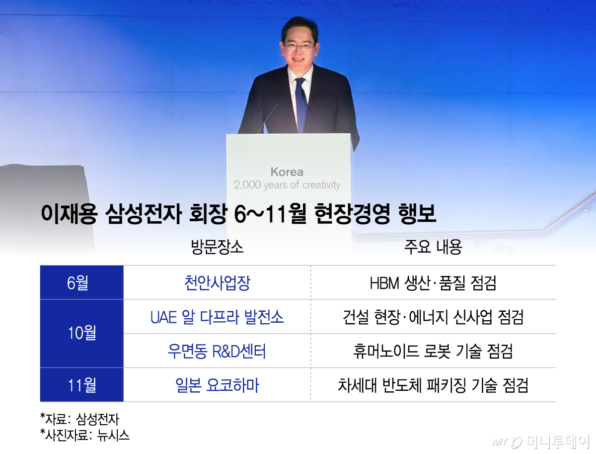
Samsung Electronics Chairman Lee Jae-yong is continuing his on-site management while accelerating efforts to strengthen competitiveness in advanced semiconductor packaging. Despite concerns about the profitability of the AI (artificial intelligence) industry and talk of an investment bubble, as well as anxieties over strengthened AI regulations following the Democratic Party's victory in the U.S. midterm elections, he appears undeterred.
It is interpreted that he is moving forward with proactive investment and technology acquisition on the firm conviction that the major trend of industrial restructuring centered on AI is irreversible.
According to semiconductor industry sources on Thursday, while market caution is growing over the profitability of the massive funds being poured into AI infrastructure, the industry's growth momentum is expected to continue.
The spread of AI services is causing data throughput and computational demand to increase geometrically. Market research firm Gartner estimates that global AI spending this year will reach $2.6705 trillion (approximately 3,585 trillion won), a 49.5% increase from the previous year. This is the backdrop for why proactive investment to prepare for high-performance semiconductor demand is becoming important, regardless of short-term market volatility.
As demand for AI semiconductors expands, technology competition to enhance performance is also changing. Circuit miniaturization remains important, but as processes become more advanced, development difficulty and cost burdens increase.
In particular, even if the computational capability of an AI accelerator's GPU (graphics processing unit) increases, overall performance is limited if data cannot be supplied quickly enough from HBM (high-bandwidth memory). This is why advanced packaging, which densely connects different chips such as GPUs and HBM to improve data transmission speed and power efficiency, has emerged as a core technology.
For Samsung Electronics, these changes represent both an opportunity and a challenge to consolidate business capabilities. The company possesses all the elements: memory for producing HBM, foundry for manufacturing logic semiconductors for AI accelerators, and advanced packaging operations.
However, individual technologies alone do not guarantee competitiveness. It must secure designs that consider inter-chip connections, heat generation, and power consumption, as well as the performance and mass production yield required by customers. The key is linking these capabilities into product competitiveness.
To translate its packaging capabilities into actual mass production competitiveness, Samsung Electronics is pursuing both production facility investment and advanced technology development in parallel. In the Chungcheong region, it is expanding the HBM back-end process mass production base, while overseas, it is securing new materials and process technologies.
Following his inspection of the HBM situation in Cheonan in June, Lee has also taken direct charge of new production facility investment through the groundbreaking ceremony in Onyang.
Overseeing overseas hubs is in the same context. Chairman Lee's visit on the 1st to the Advanced Packaging Lab (APL), an advanced packaging research hub in Yokohama, Japan, was also to inspect the status of this technology development.
Samsung Electronics plans to invest 40 billion yen (approximately 350 billion won) over five years starting from 2024 to research next-generation technologies such as wafer bonding and glass substrates at the site. The plan is to leverage Japan's strong materials, components and equipment ecosystem to secure the packaging technology needed for future high-performance semiconductors.
Lee's consecutive on-site visits are interpreted as moves to simultaneously secure production capacity and next-generation technologies in preparation for the long-term growth of the AI industry. Since semiconductor equipment investment and research and development take considerable time, the strategy is to build the foundation ahead of market expansion.
A similar trend is detected not only in semiconductors but across all next-generation growth engines. Lee, who marked his fourth anniversary as chairman last month, also inspected the status of humanoid robot technology development at the R&D center in Umyeon-dong, Seoul, continuing on-site management to secure next-generation growth drivers.
An industry official said, "Lee's increased presence at business sites is meant to reinforce vigilance and renew the company's resolve, much like late Samsung Chairman Lee Kun-hee, who constantly emphasized the need to prepare for crises. The goal is to avoid becoming complacent amid the semiconductor boom and to make a firm commitment to securing leadership in next-generation semiconductor technologies through proactive investment."

 in INDUSTRY
