

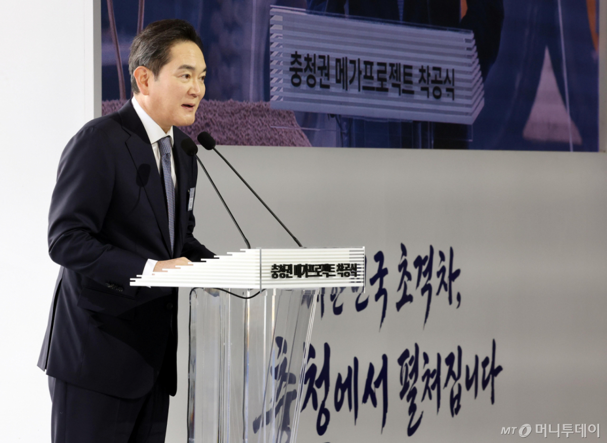
Samsung Electronics Chairman Lee Jae-yong said at a groundbreaking ceremony for a mega-project in the Chungcheong region on Thursday that the Onyang campus, once focused on assembling and testing conventional semiconductors, would be transformed into a state-of-the-art hub for high-bandwidth memory (HBM), the core of AI semiconductors.
Speaking at the groundbreaking ceremony at Samsung Electronics' Onyang campus in Asan, South Chungcheong Province, Lee said, "Until just 40 years ago, all you could see here were barren hills and unpaved roads. Today, it has become an advanced factory where semiconductors, the rice of industry, are assembled, tested and completed. With today's groundbreaking ceremony, we promise another leap forward."
He then expressed his agreement with the government's direction in promoting the mega project. Lee said, "The President has emphasized at every mega project review meeting that this is a decisive moment when the global economic landscape is being shaken." He stated, "As the President put it, I believe the mega project is not merely an industrial strategy but a historic challenge to redraw the future of the Republic of Korea."
Lee said, "I am confident that if the central and local governments, along with businesses, pool their efforts under the President's leadership, we can create a turning point for a great national leap." He added, "With a greater sense of responsibility, we will actively promote mega projects not only in the Chungcheong region but also in the Honam and Yeongnam regions to build an irreplaceable success story for the Republic of Korea."

 in INDUSTRY
