


SK Hynix completed the world's first development of HBM4 last September and entered the Yangsan phase. This memory, which is used in Nvidia's next-generation graphics processing unit (GPU), stacks 16 DRAM chips into a single unit; it is a highly complex process where even a single defective chip among the 16th requires discarding the entire finished product. Since unfiltered defects accounting for just 1% can reduce final yield by more than 10%, it is essential to thoroughly inspect each chip for defects before the stacking process.
FormFactor (FORM), a U.S.-listed NASDAQ company, is currently one of SK Hynix's key partners and maintains a close relationship in the HBM testing sector. In June this year at the SWTest (Semiconductor Wafer Test Conference) held in California, the two companies jointly announced test technologies for next-generation HBM.
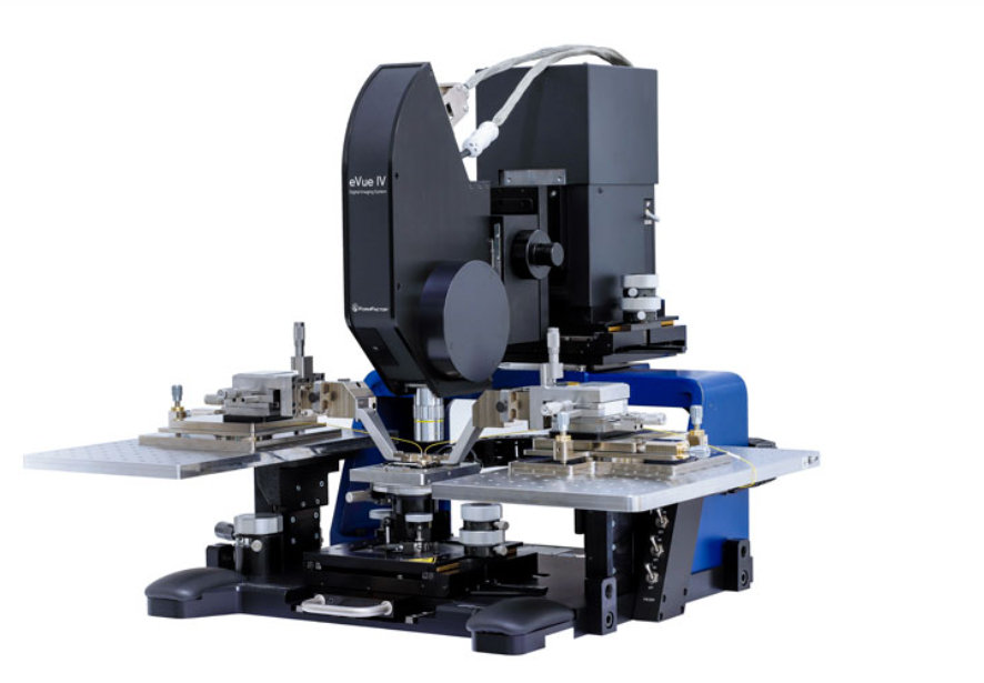
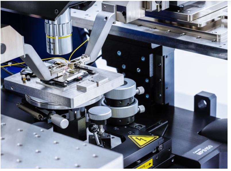
There is a device called a probe card, which checks whether electricity flows properly by simultaneously pressing tens of thousands of needles thinner than human hair onto semiconductor chips on wafers. FormFactor is the world's No. 1 company in this field. FormFactor presented empirical results showing that its HBM probe card with 60,000 needles maintained alignment even during tests involving extreme temperature fluctuations from high to low heat.
The company, headquartered in Livermore, California, derives 30 percent of its revenue from SK Hynix. In addition, it counts six major semiconductor firms—NVIDIA, TSMC, Samsung Electronics, Micron, and Intel—as customers, each accounting for more than 10 percent of total sales. The stock price has tripled over the past year, reaching a market capitalization of $10.1 billion (13.8 trillion won, based on an exchange rate of 1,365 won per dollar).
There is a reason why the form factor is called the gateway to wafer inspection. Every time a foundry or memory company designs a new chip, it must create a new probe card that precisely matches the chip's electrode array; no universal product exists. Advanced cards, which cost between $500,000 and 0.2 billion won (680 million to 2.7 billion won) per unit, wear out after hundreds of thousands of contacts, and if the chip design changes, a new card must be made again. Like photomasks, they are consumables sold repeatedly. In addition, HBM requires three times as many probe cards as standard DRAM. As stacking height increases and chips grow larger, inspection demand rises accordingly.
The person who established the form factor is Igor Khandros, a Ukrainian immigrant. He studied metallurgical engineering at Kyiv Polytechnic Institute and worked as an engineer at the Kyiv Casting Research Institute before moving to the United States in 1979. After earning a doctorate in metallurgy from Stevens Institute of Technology in New Jersey, he joined IBM's Yorktown Research Center in 1986, where he was responsible for semiconductor packaging technology that attaches chips to substrates and creates electrical connections. In 1990, he also co-founded Tessera, a company specializing in chip-scale packaging.
Candros focused on the issue of inspection sequence. Semiconductors manufacture hundreds or thousands of chips simultaneously on a single wafer, but at that time, it was only possible to identify defective chips after cutting and packaging them. This meant incurring full packaging costs for chips that were ultimately discarded. To inspect before cutting, needles had to be placed against the chip electrodes, but as electrodes became smaller and more numerous, human placement of individual needles reached its limit.
Candros solved this problem with MicroSpring technology, which uses semiconductor processes to stamp the needle itself. The method creates tens of thousands of micro-springs at once, similar to printing a photograph, and aligns them with the wafer electrode array. Due to its spring structure, it does not break when pressed and can bounce back hundreds of thousands of times. He established FormFactor in Elmsford, New York, in April 1993, and moved the headquarters to Livermore in 1995.
Sales in the first year were $1.1 million (15 billion won), with Intel and Samsung Electronics as early customers. More David, IVP, and Morgan Stanley invested in sequence. The company posted its first profit in 2000, and in 2001, sales reached $73.4 million (1 trillion won), ranking it number one globally in probe cards. It went public on the NASDAQ in June 2003, with shares rising 36% on the first day at an offering price of $14. Kandros left behind a portfolio of 220 patents.
The peak period did not last long. FormFactor sued a Korean probed card company for patent infringement at Seoul Southern District Court in 2004 and filed a lawsuit in an Oregon court in the United States in 2005, but lost both cases. In 2007 and 2008, the Supreme Court of Korea ruled that the core claims of FormFactor's Korean patents were invalid, and the U.S. International Trade Commission (ITC) issued a similar decision. As patent barriers crumbled, Samsung Electronics and SK Hynix volumes began to flow out to competitors in South Korea and Japan.
Candros stepped down as CEO in 2008 and left the company in 2009. For the next two years, the company endured turmoil with three different CEOs, and its stock price fell to $3.70 in November 2012, just one-quarter of its listing price. The company began to recover in October 2012 when it acquired competitor Microprobe for $100 million (136.5 billion won) in cash and $16.8 million (22.9 billion won) in stock. This added logic semiconductor probe cards to the company's business, which had been heavily focused on DRAM. Mike Sleser, who was CEO of Microprobe, became CEO of FormFactor in 2014.
He earned a Ph.D. in aeronautics and physics from Caltech and worked at inspection equipment company KLA. Slessor acquired Cascade Microtech for $352 million (480 billion won) in 2016, adding the research laboratory inspection system business, and subsequently acquired FRT, HPD, and Keyphotonics to expand into optical communication inspection. Currently, about 80% of FormFactor's revenue comes from probe cards, with the remainder generated from research laboratory and Yangsan inspection systems.
The competitiveness of FormFactor lies in the precision of its needles. Advanced logic and HBM require electrode spacing of less than 40 micrometers (㎛), which cannot be addressed by human-placed cantilever needles; instead, ultra-precision miniature machines (MEMS) needles manufactured through semiconductor processes are required. FormFactor possesses this process in-house. A single DRAM card can contain up to 100,000 needles, while GPU cards must withstand speeds of 448Gbps per lane and power levels exceeding 4kW. The company addresses this market with two platforms: Apollo for logic applications and SmartMatrix for DRAM and HBM applications. SmartMatrix is a technology that contacts the entire wafer at once to reduce inspection time, and it was announced during the second-quarter earnings announcement that two customers have adopted it for HBM4. Since its first shipment in 2012, HBM probe cards have surpassed their 1,000th shipment in 2025 and exceeded the 1st,500th shipment this year.
The reason HBM testing is particularly demanding lies in heat. HBM consists of micro-bumps, filler materials, and molding resins layered between DRAM chips, each with different coefficients of thermal expansion. As the device undergoes alternating high-temperature and low-temperature tests, electrode positions shift minutely, causing current to concentrate in specific areas. If a probe needle misses an electrode, it may result in discarding functional chips as defective or failing to identify actual defects.
The form factor thermal simulation model (FTSM), jointly announced by SK Hynix and the company in June this year, is a technology that calculates how much a card will warp when temperatures change and pre-adjusts needle positions during the manufacturing stage. It uses heat-resistant materials and has introduced a new cooling system instead of relying on heating methods. Validation using a 60,000-needle card confirmed that alignment was maintained at both high and low temperatures, with predicted values matching actual measurements. The form factor received SK Hynix's Best Partner Award in 2024 and ranked first globally in two categories — test subsystems and specialized equipment — in a supplier customer satisfaction survey conducted by TechInsights, a semiconductor research firm, against semiconductor manufacturers last May. This marks the company's 13th consecutive year ranking first in the testing category.
The reason customers seek a form factor is not solely precision. Probe cards are custom-made for each chip design, requiring responses to design changes within three to six months. In contrast, the form factor maintains design and production bases in Livermore and Oregon, while operating local support teams in South Korea, Taiwan, Japan, and Singapore. This approach involves working alongside chip companies' design teams from the initial silicon validation stage all the way through to Yangsan. In January 2025, strategic partnerships were also established with Advantest, the world's leading test equipment provider, and Technoprobe, the second-largest probe card manufacturer. The goal is to optimize test equipment and probe cards as a unified package to reduce customers' inspection costs.
The growth axis in the inspection system sector is optical communication packaging (CPO). As electrical wiring between AI accelerators hit a wall of speed and power, a method emerged to attach optical devices right next to chips for light-based communication, but inspection here also posed a problem. Inspecting after packaging an optical device means discarding an entire expensive GPU package for just one defect. The company first shipped the Triton equipment in 2025 at Yangsan, which performs simultaneous light and electrical testing at the wafer stage. The company explains that this method reduces inspection costs per good unit to as low as one-fifth of post-packaging inspection. This is built on experience supplying more than 100 units since launching the world's first silicon photonics inspection machine in 2017.
The probe card market is estimated to reach $2.8 billion (3.8 trillion won) in 2025 based on form factor. The second-ranked company, Italy's Techno Probe, recorded revenue of €628.4 million in 2025, holding a 34% share in the logic market and 60% in vertical MEMS. Test equipment firm Teradyne holds a 10% stake in the company. The landscape is such that form factor leads in DRAM and HBM, while Techno Probe leads in logic. Japan's MJC focuses on memory niche markets, and Taiwan's MPI handles the mid-to-low price segment. In Korea, domestic substitution is underway.
Due to this structure, the performance of Form Factor is directly tracking the pace of the transition to HBM4, according to global investment research firm Oryon Research. Second-quarter (announced on July 29) revenue reached $258.2 million (352 billion won), a 31.9% increase year-on-year, marking a record high for the quarter. The adjusted gross profit margin rose to 53.3%, up nearly 15 percentage points from 38.5% a year ago, while adjusted earnings per share (EPS) of $0.82 was three times that of the previous year. Notably, revenue grew by more than 30% over the past four quarters alongside a sharp surge in profit margins, indicating how rapidly the company has entered a steep growth phase.
By business segment, DRAM probe cards reached $82.9 million (113 billion won) in the first quarter, a 70% increase, with two-thirds of that attributed to HBM applications. Foundry and logic probe cards rose 30% to $111.2 million (152 billion won). The inspection systems segment surged 74% to $48.5 million (66 billion won) in the second quarter. CPO inspection revenue is expected to exceed the initial forecast of 0.1 billion won to 0.2 billion won by the third quarter.
Annual revenues are as follows: △2024: $763.6 million (₩1.42 trillion), △2025: $785 million (₩1.71 trillion), and △first half of 2026: $484.3 million (₩66.1 billion). The third-quarter guidance calls for revenues of 2.7 billion won (₩36.9 billion), an adjusted gross profit margin of 54%, and EPS of $0.86. Last year's full-year EPS was $1.30, but this figure will be surpassed within just two quarters this year. With cash and marketable securities totaling $345.7 million (₩4.72 billion) and long-term debt at only $10.5 million (₩143 million), the company is effectively operating without any borrowing.
The company presented its 2030 targets at an investor presentation held on May 11 in New York on the NASDAQ. The core goals include revenue of $1.6 billion (2.18 trillion won), double that of 2025; a gross profit margin of 55%; EPS of $5; and operating profit growth of five times. These targets are based on increased HBM stacking layers, rising power and speed demands for GPUs and custom AI chips, and the maturation of the CPO inspection market. The company has identified its target market as growing from $3.1 billion in 2025 to $4.5 billion by 2030, representing an annual growth rate of 8%. The company plans to grow its own revenue at twice that pace, aiming to capture a market share of up to 36%. To achieve this, the company is constructing a new factory in Farmers Branch, Texas. Production is scheduled to begin by the end of this year, with Yangsan output to increase in the first quarter of next year, and contributions to profit margins expected from 2028 onward. Equipment investment for this year is estimated at $140 million to $170 million (190 billion to 230 billion won). As of the end of last year, the company employed 2,153 people: 1,298 in production and 422 in research and development. The management team is composed of individuals with backgrounds from KLA, ASML, AMD, Onto, and Texas Instruments.
The average target price set by 11 Wall Street analysts is $127.45. The closing price on the 25th, at $129.69 (177,000 won), has already surpassed this average target. The stock price rose to $160.27 on June 30 before falling by 19%. The company stated during its second-quarter conference call that supply chain constraints have halted production capacity expansion and prevented it from fulfilling all new CPU customer orders. This means growth will be constrained by production capacity until the Texas plant begins full operations in 2027.
The variables that will determine the future direction of stock prices are the fourth-quarter guidance to be released in third-quarter earnings at the end of October and the shipment speed of HBM4 from SK Hynix and Micron. Probe card orders are typically placed one quarter ahead of memory shipments.
◇ Major Milestones of Form Factor
Established in April 1993 by Igor Kandruss in Elmsford, New York. Relocated to Livermore, California, in 1995.
Launched the needle microspring made through semiconductor processes in 1995; first sales reached $1.1 million.
With 2001 sales of $73.4 million, it ranked first in the world for probed cards.
Listed on the NASDAQ in June 2003 with an initial public offering price of $14, rising 36% on its first day.
2004–2010 Korea-Picom vs. Japan-MJC patent lawsuit; Korean Supreme Court ruled patents invalid; no ITC violation found
Candros retired in 2009. In November 2012, the stock price hit a historic low of $3.70.
Acquired Microprobe in October 2012; entered the logic probe card market. First shipment of HBM probe cards.
Mike Slessor assumed the role of CEO in 2014. Cascade Microtech was acquired in 2016.
In the first quarter of 2026, SK Hynix accounted for 29.5 percent of revenue share and became Nvidia's first customer to reach a 10 percent threshold.
Investor presentation scheduled for May 2026, targeting $1.6 billion in revenue and $5 EPS by 2030
June 2026: SK Hynix and HMB probe card thermal correction technology jointly announced
Q2 2026 revenue of $258.2 million, marking the fourth consecutive quarter with 30% growth

 in STOCK


