

Samsung Electronics has broken ground on an advanced packaging plant for high-bandwidth memory (HBM) in Onyang, Asan, South Chungcheong Province, and will bring forward its operational start date by approximately one year. To respond to the growing demand for memory semiconductors (hereinafter referred to as memory) for AI (artificial intelligence) servers, the company aims to secure back-end production capacity early and invest 4.6 trillion won to transform the Onyang site into a core HBM production hub.
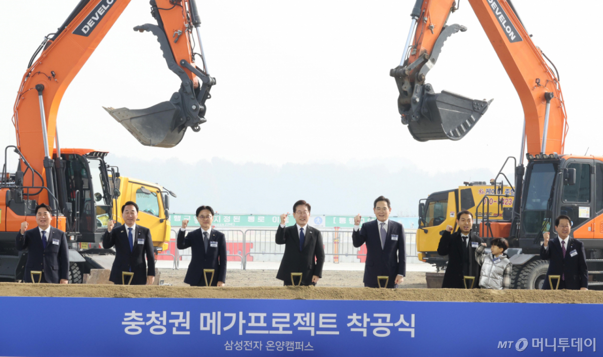
On the morning of the 12th, Samsung Electronics held the "Chungcheong Region Mega-Project Groundbreaking Ceremony" at the Onyang site, attended by President Lee Jae-myung and Chairman Lee Jae-yong of Samsung Electronics, among others. This event marks the first project under the government's three major mega-projects.
In his welcome address, Chairman Lee stated, "With today's groundbreaking ceremony, we pledge another leap forward," emphasizing that "this site, which has centered on processes for simply assembling and inspecting general semiconductors, will transform into a cutting-edge HBM hub, the heart of semiconductors."
With this groundbreaking, the Onyang site is set to become a core advanced HBM packaging hub 35 years after it began as a semiconductor assembly and inspection line in 1991. Samsung Electronics plans to sequentially invest a total of 4.6 trillion won (6 trillion won for plant construction and 40 trillion won for advanced equipment) at the Onyang site to build five HBM fab lines and expand the site's total floor area from the existing 270,000 square meters to 420,000 square meters.
Chun Young-hyun, President of Samsung Electronics and Vice Chairman of the DS (Device Solutions) Division, who presented a status report, indicated that the operational start date for the five lines at the Onyang site would be June 2028, one year ahead of the original plan. The new plant, currently undergoing foundation work, will feature cleanrooms spanning three floors with a total area of approximately 31,000 square meters. The investment amount for the new plant is approximately 1.3 trillion won.
The reason Samsung Electronics is rushing to bring forward the operational start date is the surge in demand for server memory. In its third-quarter earnings announcement last month, Samsung Electronics disclosed that it had completed negotiations on HBM supply volumes for 2027, but that requests from customers for additional volume increases are continuing. In particular, the company forecast that supply shortages would persist until 2028. Since HBM is a product made by stacking and connecting multiple memory chips vertically, expanding chip production alone has limits in increasing supply unless supported by back-end packaging facilities.
The growth of the advanced packaging market, which determines HBM performance and production capacity, is also steep. Market research firm Yole Group forecasts that the high-performance advanced packaging market will grow at an annual average rate of 27% from 2025 to 2031, surpassing $51 billion in 2031. Samsung Electronics' strategy is to consolidate its capabilities in memory, foundry (semiconductor contract manufacturing), and packaging to enhance its mass production competitiveness in HBM.
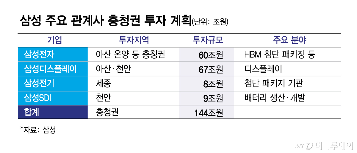
Meanwhile, investments by major affiliates in the Chungcheong region are also gaining momentum. Samsung Display (Asan and Cheonan, 67 trillion won) and Samsung Electro-Mechanics (Sejong, 8 trillion won) began construction of new plants last month, while Samsung SDI (Cheonan, 9 trillion won) is operating battery production and development facilities. Including Samsung Electronics (60 trillion won), the total investment in the Chungcheong region amounts to 144 trillion won.
Samsung plans to use its investments in the Chungcheong region as a springboard to support the expansion of mega-projects to other regions. Chairman Lee emphasized, "The mega-project is not merely an industrial strategy but a historic challenge to redraw the future of South Korea," adding, "With a greater sense of responsibility, we will actively promote mega-projects in the Honam and Yeongnam regions as well as here in Chungcheong for the success story of an irreplaceable South Korea."

 in INDUSTRY

