

[For more diverse corporate information on startups, you can view it on the Unicorn Factory Big Data Platform 'Data Lab' .]
The semiconductor industry has improved performance by making transistors (semiconductor devices that function as electrical switches and voltage amplifiers) smaller. This involves integrating more transistors into a single chip to increase computing speed while reducing power consumption.
However, as semiconductor processes have shrunk to below the 2nd-nanometer (nm) level, the question of "what to make them with" has become an important issue, going beyond "how small can they be made."
This is because when the 'channel,' which is the pathway for current flow inside a transistor, becomes thin at the atomic level, it becomes difficult to precisely control the current using existing silicon materials. Problems such as increased leakage current and heat generation, as well as degraded device performance, can also occur.
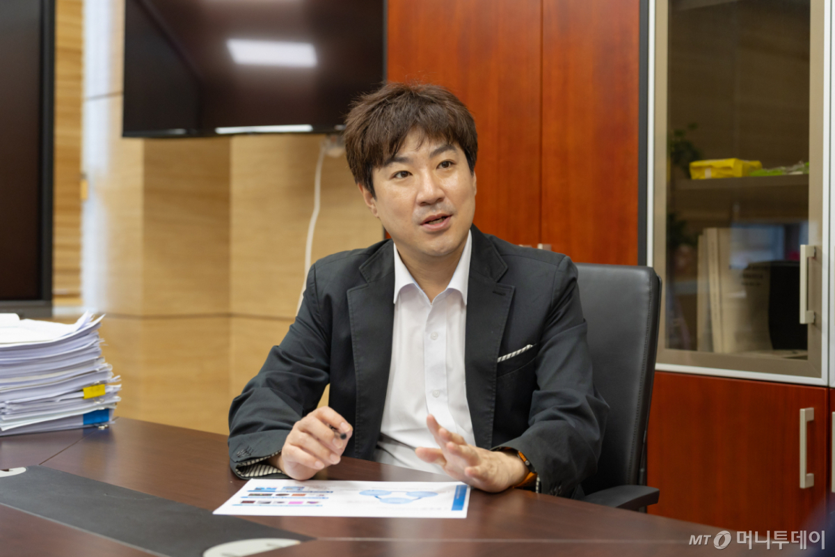
Professor Im Hyeon-seop of the Department of Chemistry at Gwangju Institute of Science and Technology (GIST) stated, "As semiconductor processes continue to shrink, there is a physical limit to improving performance with silicon," adding, "Ultimately, we are in a state where the material itself used for the channel must be changed to a better one."
2D Semiconductors as Silicon Alternative… Key Is Large-Area and Uniform Production
Candidates to replace or complement silicon include 'two-dimensional (2D) semiconductors' that are thin at the atomic layer level. A representative material is molybdenum disulfide (MoS₂). MoS₂ has a sandwich structure where molybdenum atoms are placed between sulfur atoms. It possesses a 'band gap,' which is the energy interval that allows current to be turned on and off, even though its thickness is less than 1 nm.
Graphene is also a representative 2D material, but it has almost no band gap, limiting its use as a digital semiconductor channel. On the other hand, transition metal dichalcogenides (TMDs) such as MoS₂, tungsten disulfide (WS₂), and tungsten diselenide (WSe₂) maintain their semiconducting properties even at atomic layer thicknesses.
It is explained that being thin makes it advantageous for the gate to control the current inside the channel. By stacking different 2D materials layer by layer, semiconductor functions can be integrated in three dimensions, going beyond the existing silicon-based planar structure.
The potential of 2D semiconductors has been confirmed early on, but there were not few barriers to overcome before applying them to industrial sites. One of the biggest problems is securing uniform quality over large areas (wide surface area).
Using mechanical exfoliation methods that peel off layers with adhesive tape can yield 2D materials with excellent crystallinity. However, the size is only on the order of a few micrometers (µm), making it difficult to apply to wafers for mass production.
Using chemical vapor deposition (CVD) allows very thin semiconductor films to be grown on wider substrates. The problem is that slight differences in the supply amount of raw materials, the surface state of the substrate, temperature, and pressure can cause variations in the material's thickness, crystal orientation, and quality.
Professor Im stated, "Making high-quality material once in a laboratory is a completely different issue from repeatedly producing the same quality on a production line," adding, "In industry, 'reproducibility,' where quality is consistent for each wafer and at each position on the wafer, is as important as top performance."
He continued, "We are continuously developing technology to synthesize 2D semiconductor materials well and on a large scale," adding, "The key is not just making good material once, but understanding why it is made that way to improve reproducibility."
Beyond 'Shake and Bake'… Improving Reproducibility by Revealing Synthesis Principles
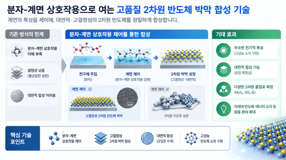
Professor Im presented 'High-Quality 2D Semiconductor Thin Film Synthesis Technology' as a solution. The core is to uniformly synthesize next-generation semiconductor materials that are thin at the atomic layer level over wide areas.
While existing methods used a 'shake-and-bake' technique of putting various raw materials and substrates into equipment, changing conditions, and checking results, he approached it by chemically elucidating and controlling the interaction between precursor (raw material that is transformed into the final substance through chemical reaction) molecules and the substrate interface.
Professor Im stated, "It goes beyond recording under what conditions a good film was produced; it involves elucidating at the molecular level why crystals grew in one direction under those conditions and why the thickness varied."
Professor Im's research team utilized inorganic molecular precursors called molybdenum oxychloride (MoOCl₄) and tungsten oxychloride (WOCl₄), instead of solid raw materials such as molybdenum trioxide (MoO₃) and tungsten trioxide (WO₃) that were mainly used previously.
It is difficult to precisely control how much solid raw material vaporizes during the heating process and reaches the substrate. On the other hand, if molecular precursors are made into gas, the input amount can be adjusted more finely using flow controllers and fine-adjustment valves.
Professor Im compared it to "using measuring tools to repeatedly produce the same taste instead of adding ingredients by eye when cooking," stating, "We elucidated through experiments and calculations the principle that 'chemical adsorption' between the precursor and substrate, and 'physical adsorption' between the precursor and already grown film, operate differently depending on pressure."
Professor Im emphasized that grasping the fundamental principles of synthesis is a differentiator for his research team. He explained that although overseas researchers, including those in China and Taiwan, are quickly releasing new large-area synthesis methods, it is difficult to secure the reproducibility required in industrial sites with results obtained only from specific equipment or conditions.
He stated, "You must know how molecules and substrates interact with each other so that you can redesign the process even when conditions change," adding, "Understanding of principles is also necessary to expand the technology to other substances, not just specific 2D materials."
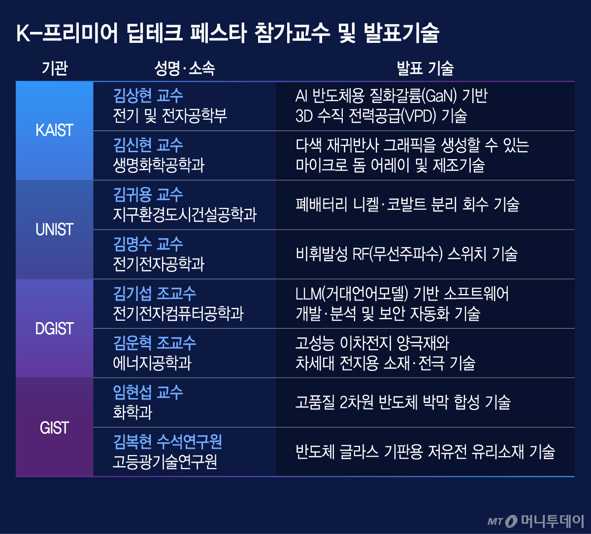
Professor Im will introduce related technologies at the '2026 K-Premier Deep Tech Festa' (Registration: https://vvd.bz/buvX), which will be held on the 29th at the Plus Stage in Hall B of COEX in Samsung-dong, Seoul. He revealed, "I hope to collaborate not only with large companies like Samsung Electronics and SK Hynix but also with SMEs (small and medium-sized enterprises) developing semiconductor materials."
<Registration for 'K-Premier Deep Tech Festa (Technology Transfer · Commercialization)' >
- Date: October 29, 2026 (Thu), 1:00 PM
- Location: PLUS STAGE, Hall B, COEX, Samsung-dong, Seoul
- Participants: Companies considering technology transfer, joint research, and new businesses; family companies of government-funded research institutes; investment firms
- Participation Fee: Free (Pre-registration required)
- Hosts: Ministry of Science and ICT, KAIST, GIST, DGIST, UNIST, MoneyToday Unicorn Factory
- Sponsors: Korea Institute of Science and Technology Information (KISTI), Commercialization Promotion Agency for R&D Outcomes (COMPA)
- Application: https://vvd.bz/buvX
[MoneyToday startup media platform 'Unicorn Factory' ]

 in FUTURE


