

Hanmi Semiconductor is expanding its business scope beyond TC bonders (thermocompression bonding equipment) for HBM (high-bandwidth memory) to advanced packaging equipment for system semiconductors. The company has begun supplying new equipment to a customer in Taiwan and established a local subsidiary in the United States, accelerating the expansion of its product lineup and customer base.
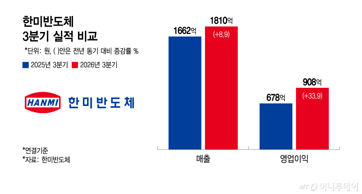
Hanmi Semiconductor said Friday that it posted revenue of 181 billion won and an operating profit of 90.8 billion won in the third quarter this year, representing increases of 8.9% and 33.9%, respectively, compared to the same period last year.
The operating profit margin was 50.2%, up 9.4 percentage points from the same period last year. Despite a decline in exchange rates and the deferral of some equipment revenue to the fourth quarter, the company achieved simultaneous growth in scale and improved profitability, centered on high-value-added equipment such as TC bonders for HBM.
Product diversification is translating into equipment supply in the global market. In September, Hanmi Semiconductor began supplying 2.5D packaging equipment that integrates GPUs (graphics processing units) and HBM among others into a single unit to a foundry customer in Taiwan. The equipment reportedly passed the customer’s mass production standards and has been deployed on actual production lines.
Hanmi Semiconductor also secured additional orders for FC (flip-chip) bonders from its Taiwanese customer. Separately, last month, the company shipped its FC Bonder 75, a large interposer processing equipment that connects different semiconductor chips, to a global customer for the first time, expanding supply to high-performance AI semiconductor packaging lines.
While existing TC bonders for HBM focused on memory stacking, the new equipment is characterized by extending its application scope to system semiconductor packaging processes. This enables the company to respond not only to HBM capital expenditures by memory manufacturers but also to packaging investments by foundries and back-end process companies.
In line with the diversification of its equipment portfolio, Hanmi Semiconductor is accelerating the expansion of its global sales network. The company established a local subsidiary, "Hanmi USA," in San Jose, California, this month. Given that its overseas revenue share has averaged over 72% for the past 15 years, the company plans to strengthen local technical support and pursue new customers using the U.S. subsidiary as a hub.
Indeed, related investments are continuing locally in the United States, including SK hynix’s HBM packaging plant in Indiana (targeting operation in the second half of 2028) and Amkor Technology’s advanced packaging facility in Arizona. Hanmi Semiconductor is expected to actively seek equipment supply opportunities for new plants in the U.S., leveraging its TC bonders for HBM stacking and FC bonders for advanced packaging.
Hanmi Semiconductor is projected to record its highest-ever revenue on a quarterly basis, as deferred equipment revenue from the fourth quarter is recognized and supplies to overseas customers increase. Its annual revenue is also likely to set a new record for the third consecutive year, following 2024 and 2025.
A company official said, "Using Hanmi USA as a hub, we will strengthen local technical support and the acquisition of new customers to aggressively target the emerging U.S. advanced packaging market."
The official added, "Alongside TC bonders for HBM, we will supply mass-production versions of various AI packaging TC bonders and FC bonders, Micro Solder & Vision Placement (MSVP), and EMI (electromagnetic interference) shield equipment for aerospace and smart devices to customers, sustaining medium- to long-term growth in scale."

 in INDUSTRY
