

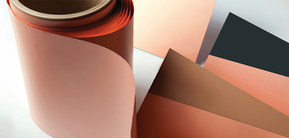
Doosan Group is moving into copper-clad laminate (CCL) for semiconductor packages in Yangsan, which is 5μm (micrometers) thinner than existing products. As CCL becomes thinner, the thickness and volume of semiconductor package substrates decrease accordingly, enabling not only miniaturization but also higher integration density.
According to industry sources on the 24th, Doosan Electronics BG (hereinafter referred to as Doosan) has proactively secured technology that significantly reduces the thickness of the insulating layer (PPG) in CCL used for memory semiconductor package substrates from an average of 18μm down to 13μm and is preparing for production in Yangsan. One micrometer (μm) equals one-millionth of a meter; 13μm is approximately one-fifth the thickness of a human hair. CCL is constructed by placing PPG between layers of copper foil. To reduce the thickness of CCL, Doosan Electronics BG must control the PPG layer. The thinner the PPG becomes, the thinner the overall CCL and the resulting semiconductor package substrate can be made.
Jung Soo-im, team leader of the P&AM Development Team at Doosan Electronics BG, stated, "In the memory semiconductor substrate market, only Doosan is capable of meeting 13μm requirements." He further explained, "Optimizing the physical properties of PPG by adjusting the composition of various materials (including resin, an epoxy-based raw material), surface treatment structures, dispersion methods, and content levels is critical. Through these technological advancements, we have successfully achieved a 13μm thickness."
In this process, Doosan Electronics BG newly applied "organic filler," a plastic-based elastic powder. Previously, high-density filling technology using inorganic "silica fillers" was employed for PPG in semiconductor package substrates to prevent deformation under heat. However, as the filler content increased, adhesive strength and pattern filling ability between circuits declined, creating limitations in making PPG thinner than 13μm. Team leader Jung added, "We reduced thickness by applying special chemical treatment to the surface of organic fillers, which exhibit low coefficient of thermal expansion (Low CTE) characteristics—meaning they undergo minimal dimensional change when exposed to heat—thereby controlling particle dispersion and physical properties."

 in INDUSTRY

