

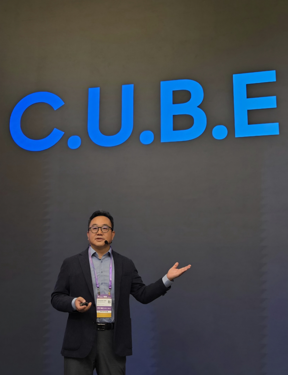
Samsung Electronics has unveiled its 'CUBE' strategy, which vertically stacks memory semiconductors (hereinafter referred to as memory) to increase capacity and bandwidth while improving power and thermal efficiency. The company plans to maintain leadership in memory technology for the AI era through the development of eighth-generation high-bandwidth memory (HBM5) and next-generation 3D memory 'zHBM'.
According to the electronics industry on the 1st, at Semicon Taiwan 2026 held in Taipei, Taiwan, Jang-seok Choi, Executive Vice President and Head of Product Planning Team at Samsung Electronics' DS Division Memory Business Unit, announced this CUBE strategy to overcome limitations in memory technology. Vice President Choi attended the 'Memory Executive Summit', a pre-event of Semicon Taiwan.
CUBE specifically refers to: △Capacity, △Optimization (Utilization), △Bandwidth, and △Power/Thermal Efficiency. Samsung Electronics aims to strengthen its leadership in memory technology by simultaneously improving these four elements based on a 3D stacking structure.
First, regarding capacity, the company will vertically expand memory to overcome constraints imposed by printed circuit board (PCB) area. While the conventional method of placing memory chips on a flat plane requires larger board areas as capacity increases, stacking chips vertically enables greater capacity within the same footprint.
Samsung Electronics is also advancing memory optimization. Vice President Choi explained, "3D is not simply about stacking; the key lies in how each layer is utilized," adding, "We are optimizing logic and memory placement to eliminate data processing delays."
The 3D stacking structure also reduces the distance data must travel. Samsung Electronics plans to build a 'vertical highway' by narrowing the distance between dies, enabling faster data movement and significantly boosting memory bandwidth.
Power consumption and heat generation issues will also be addressed. As AI accelerator performance improves, the volume of data transferred increases, leading to higher power usage and heat dissipation. Vice President Choi emphasized, "The ultimate goal of 3D is to reduce the energy required to move a single bit of data," noting, "We are maximizing performance per watt by enhancing structural efficiency."
The CUBE strategy will also be applied to next-generation HBM products. Samsung Electronics is advancing capacity, bandwidth, power efficiency, and thermal management technologies from HBM2 through HBM4E to HBM5. The developing HBM5 aims to double performance compared to HBM4E while reducing thermal resistance by 20%.
The next-generation 3D memory 'zHBM', whose concept was unveiled earlier this year, is expected to deliver eight times the general performance and three times the performance per watt compared to HBM5. Its focus is on reducing thermal resistance by 75–90%, addressing the performance limits and heat issues of existing HBM.
Samsung Electronics is also developing 'zNAND-O', a NAND flash based on 3D packaging. zNAND-O boasts ten times higher bit density than DRAM, while offering seven times greater read bandwidth and power efficiency compared to conventional NAND. Samsung Electronics plans to begin supplying samples of zNAND-O starting in 2028.
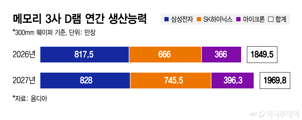
Leveraging its world-class production capacity, the company intends to respond to demand for both HBM and general-purpose memory. Omdia forecasts Samsung Electronics' DRAM production capacity this year at 8.175 million 300mm wafers annually, surpassing SK Hynix's 6.66 million and Micron's 3.66 million units.
However, as major memory manufacturers including Samsung Electronics concentrate resources on producing high-value-added products like HBM, supply of general-purpose DRAM is expected to become increasingly tight. Since HBM is manufactured by vertically stacking multiple DRAM dies, increased production requires more wafer and advanced packaging capacity. With no significant changes in overall production capacity, a larger share of HBM will reduce the available capacity for general DRAM.
Industry observers view the expansion of HBM production as a key variable affecting DRAM supply and demand next year. Some analyses suggest that DRAM supply for PCs may contract next year. As securing memory becomes more difficult, there are also signs of manufacturers opting for lower-grade DRAM in budget PC products.
DRAM prices are also fluctuating. Market research firm TrendForce predicts that contract prices for PC DRAM will rise by 18–23% in the third quarter of this year compared to the previous quarter, an upward revision from its earlier forecast of 15–20%. Last month's contract price for a 16GB DDR5 module reached $247, marking a 20.5% increase compared to three months prior.

 in INDUSTRY

