

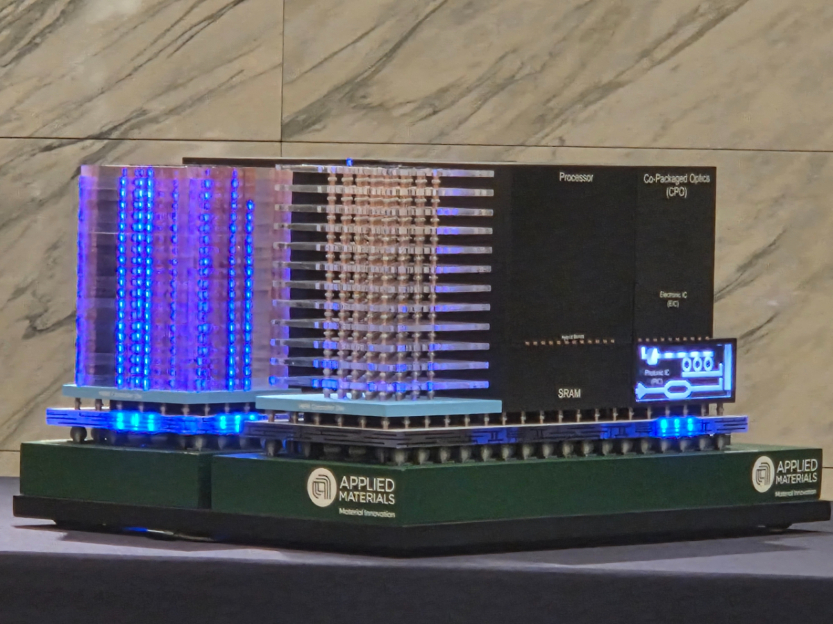
The technological leadership race in AI (artificial intelligence) semiconductors is shifting from DRAM miniaturization to stacking and connecting chips through packaging. As Samsung Electronics and SK Hynix expand their domestic and overseas production bases, securing advanced packaging technology that determines data transmission efficiency has emerged as an essential task.
According to industry sources on the 31st, Samsung Electronics and SK Hynix are actively accelerating investments in advanced packaging and expanding facilities to secure leadership in AI semiconductors. Recently, SK Hynix held a groundbreaking ceremony for an AI memory advanced packaging production base in West Lafayette, Indiana, USA, with an investment of over $4 billion (approximately 5.4824 trillion won). The company plans to begin producing next-generation HBM (High Bandwidth Memory), HBM4E (7th generation), at its Yangsan facility from the second half of 2029. Samsung Electronics is also increasing investments in packaging facilities, focusing on Chungcheong regions including Cheonan and Asan in South Chungcheong Province.
Both companies are accelerating their packaging investments because factors determining AI semiconductor performance have expanded beyond individual DRAM to include technologies for stacking and connecting chips. As AI evolves from learning-centric stages to real-time inference and decision-making, the volume of data requiring processing is surging. In this process, there is a need to improve not only DRAM performance but also data transfer efficiency to overcome the memory wall—a situation where processor computation speeds cannot keep up with memory data supply speeds.
Consequently, both DRAM and HBM packaging technologies are being advanced together. At a media briefing held at Seoul Coex today, global semiconductor equipment company Applied Materials explained that technology is evolving from expanding EUV (extreme ultraviolet) application and improving peripheral circuit performance to vertical transistor-based 4F² and 3D DRAM solutions.
As HBM stacking increases, connection technologies between chips become increasingly important. Technology is advancing from TSV (through-silicon via) and micro-bump methods to direct copper bonding using HYBE lead bonding. This aims to reduce chip spacing while improving connection density and power efficiency. In particular, 2.5D/3D integration that places memory and computing devices close together, as well as co-packaged optics (CPO) for transmitting data via optical signals, are also under development. Samsung Electronics and SK Hynix must inevitably focus not only on HBM performance and production volume but also on their technical capabilities to efficiently stack and connect chips.
These changes appear to offer new opportunities for Korea's materials, components and equipment industry. As semiconductor structures become more complex, demand grows for new materials, deposition and etching technologies, and precise measurement and inspection. Applied Materials stated that AI semiconductor demand exceeds supply, leading customers to request additional facility expansions and equipment supplies. The domestic materials, components and equipment industry also plans to expand production capacity and advance technology in line with Samsung Electronics and SK Hynix's expansion of domestic and overseas production bases.
Park Kwang-seon, CEO of Applied Materials Korea, also noted on this day that Korea's strategic importance will grow further in the AI semiconductor market centered on HBM. He emphasized, "HBM is emerging as a core critical technology for the AI ecosystem, and two out of three companies manufacturing advanced memory are located in Korea," adding, "Korea will occupy an increasingly strategic and important position going forward."

 in INDUSTRY
