

The background behind Samsung Electronics partnering with ASML, the sole provider of EUV (Extreme Ultraviolet) lithography equipment, during a semiconductor industry upheaval driven by AI is clear. The strategy is to solidify its No. 1 global competitiveness in DRAM amid upcoming ultra-fine process competition and to participate from the stage of setting standards, not merely securing equipment supply.
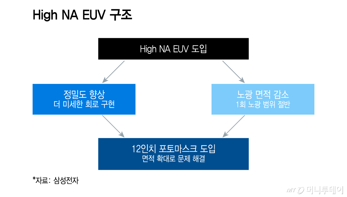
According to relevant industry sources on the 8th, the performance and productivity of semiconductors depend on how small and precise circuits can be drawn. EUV is a technology that transfers fine circuits drawn on photomasks onto wafers (thin discs used to make semiconductor chips) using light. The next-generation equipment, High NA (High Numerical Aperture) EUV, is considered essential for advanced semiconductor miniaturization because it can draw even finer circuits than existing EUV systems. It can reduce the line width of drawable circuits from 13nm (nanometers) to around 8nm, allowing devices to be made up to 1.7 times smaller and theoretically increasing density by up to 2.9 times.
The problem is that while precision improves, the area where circuits can be etched at once is halved. If the current 6-inch photomasks are used as-is, it becomes necessary to divide large circuits into multiple sections for etching and then stitch them together. Errors during this process would require rework, potentially extending production timelines and increasing costs.
The solution lies in 12-inch photomasks. Photomasks serve as a kind of "template" with the circuits to be transferred onto wafers drawn on them. Simply put, it is a concept of doubling the size of the current template, which is about 15cm, to a 30cm standard. This allows wider circuits to be etched in one go, reducing the need for segmented drawing and improving production efficiency.
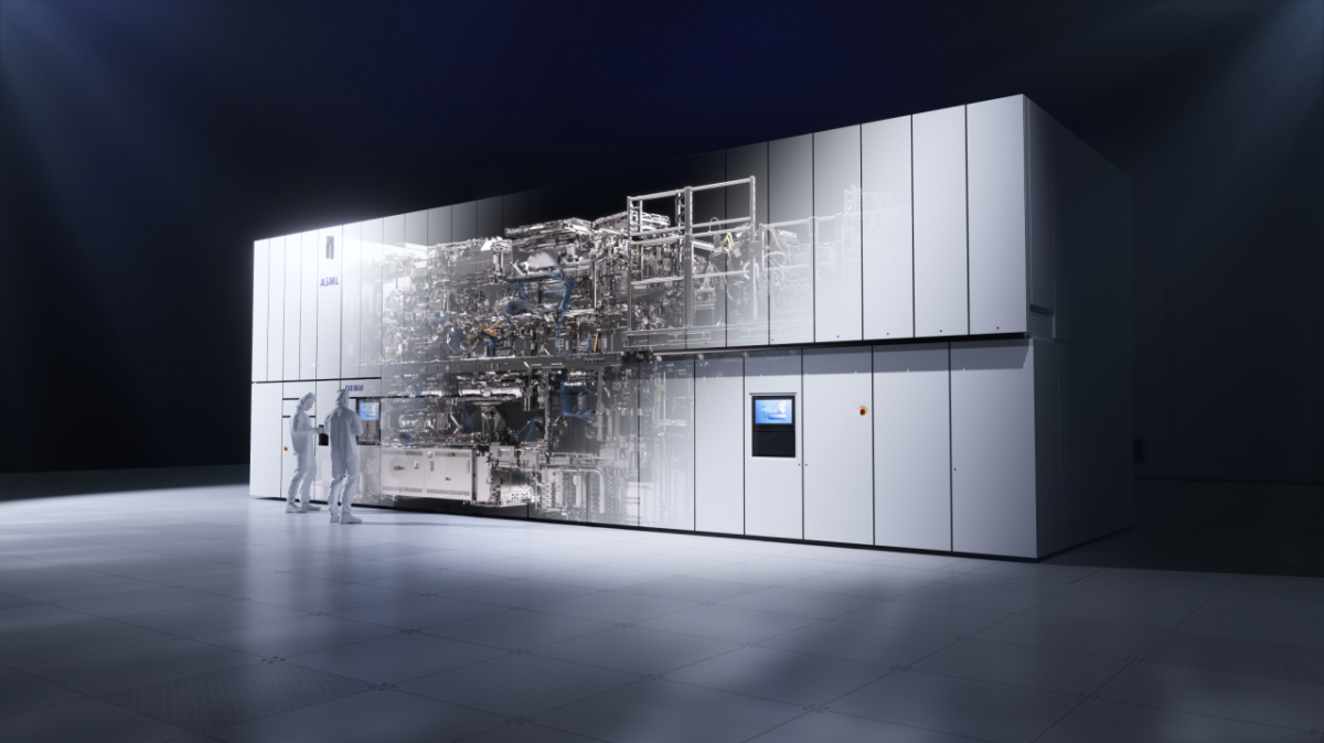
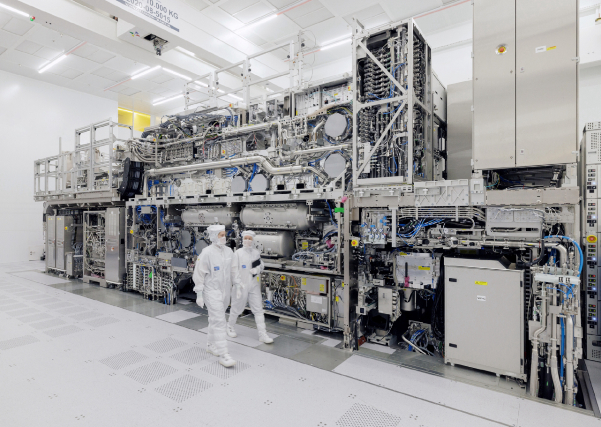
This is also why Samsung Electronics is preparing with ASML not only on equipment but also on photomask development. To apply high numerical aperture EUV to actual production lines, simply changing the equipment is insufficient. Related companies, including those producing photomasks and materials, must also develop technologies aligned with new standards. Samsung Electronics' participation from the stage of building this ecosystem appears aimed at proactively securing the technology and production base needed for applying high numerical aperture EUV to DRAM in Yangsan by 2028.
This ultimately ties directly to the production competitiveness of next-generation DRAM. As circuits become finer, existing EUV systems require multiple operations to produce the same circuit, whereas high numerical aperture EUV can reduce the number of process steps. Following its pioneering use of EUV in DRAM production in 2020, Samsung Electronics plans to secure Yangsan experience first with DRAMs applying high numerical aperture EUV. This is a strategic move to simultaneously enhance miniaturization and productivity, thereby strengthening manufacturing technology competitiveness and solidifying its leadership in the DRAM market.
In particular, synergy with ASML is expected given that Samsung Electronics is a comprehensive semiconductor company possessing both memory semiconductors (hereinafter "memory") and foundry (semiconductor contract manufacturing) capabilities. Although ASML also collaborates with TSMC and Intel, Samsung Electronics simultaneously develops and produces advanced memory and leading-edge foundry processes. It is expected to differentiate itself from competitors by being able to utilize the next-generation lithography technology and ecosystem built together with ASML across various advanced semiconductor manufacturing processes.
An industry insider stated, "Through close collaboration with global equipment company ASML, we can enhance the completion level of next-generation DRAM development utilizing high numerical aperture equipment," and added, "Accumulated operational experience with high numerical aperture equipment in the future will greatly contribute to yield stabilization and productivity improvement."

 in INDUSTRY


